Thermocouple

a thermocouple and sensor technology, applied in the field of thermocouple, can solve the problems of less accurate temperature data provided by the thermocouple, affecting the uniformity of the resulting structure on the surface of the substrate, and unusable areas on the surface of the finished substra

Active Publication Date: 2012-01-24
ASM IP HLDG BV
View PDF126 Cites 344 Cited by
  • Summary
  • Abstract
  • Description
  • Claims
  • Application Information

AI Technical Summary

Benefits of technology

[0009]In one aspect of the present invention, a thermocouple disposable within a susceptor ring is provided. The thermocouple comprises a sheath disposable within the susceptor ring. The thermocouple further includes at least one thermocouple junction located within the sheath. The thermocouple also includes at least one inner alignment feature and / or at least one outer alignment feature for positively locating or aligning at least one thermocouple junction relative to the susceptor ring.

Problems solved by technology

If the temperature varies greatly across the surface of the substrate, the deposited layer could be uneven which may result in unusable areas on the surface of the finished substrate.
Similarly, non-uniformity or instability of temperatures across a substrate during other thermal treatments can affect the uniformity of resulting structures on the surface of the substrate.
When the junction of the thermocouple is offset from the precise location during installation, the temperature data provided by the thermocouple is less accurate the farther away the junction is from the desired location.

Method used


Image

  • Thermocouple
  • Thermocouple
  • Thermocouple

Examples


Embodiment Construction

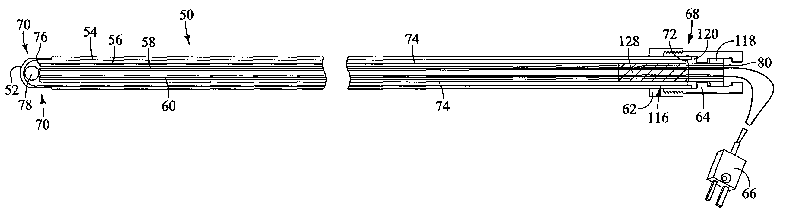
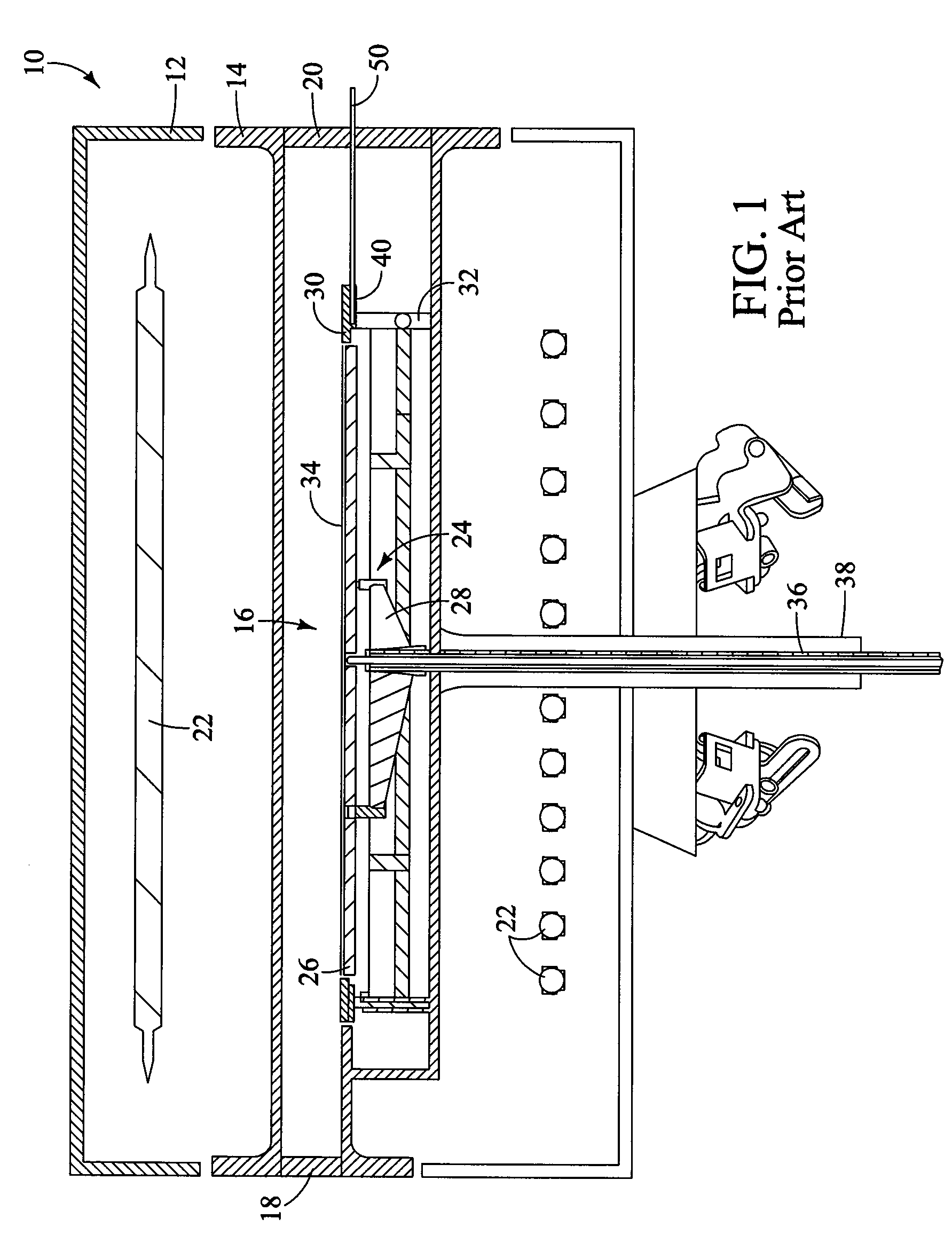
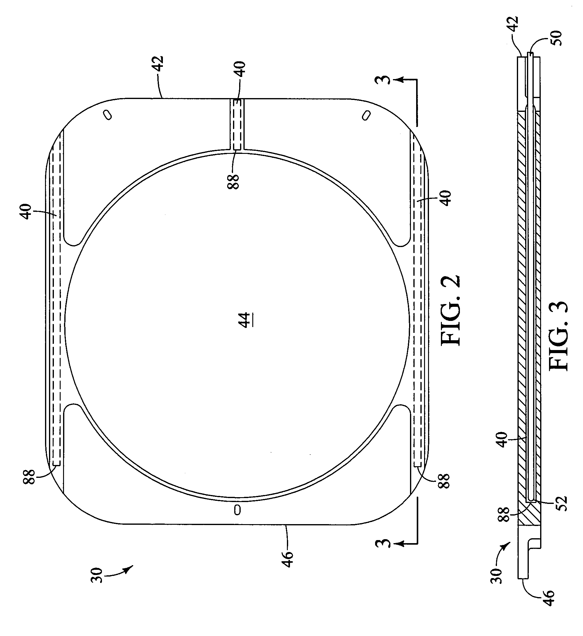
[0035]Referring to FIG. 1, an exemplary embodiment of a semiconductor processing reactor 10 generally known in the art is shown. The reactor 10 may be a configured for chemical vapor deposition (“CVD”) processes, atomic layer deposition (“ALD”) process, or any other processes for depositing thin layers of material onto a substrate located within the reactor 10. FIG. 1 illustrates a known reactor 10 typically used in the Epsilon® tools produced by ASM America, Inc. of Phoenix, Ariz. The reactor 10 of the illustrated embodiment includes a housing 12 and a cold-wall, single-substrate reaction chamber 14 located within the housing 12. However, it should be understood by one skilled in the art that the reaction chamber 14 can be of any type capable of processing substrates therein. The reaction chamber 14 defines a reaction space 16 within which chemical reactions take place. The reaction chamber 14 includes an inlet 18 through which process gases are introduced into the reaction space 1...


PUM

PropertyMeasurementUnit
temperatureaaaaaaaaaa
dimensionsaaaaaaaaaa
rotationaaaaaaaaaa

Abstract

A thermocouple having at least one inner alignment feature or at least one outer alignment feature, or a combination thereof for positively positioning and aligning at least one thermocouple junction within a bore formed in a susceptor ring of a semiconductor substrate processing reactor. The outer alignment feature is configured to positively align the junction(s) longitudinally within the bore. The inner alignment feature configured to positively position the junction(s) rotationally within the sheath of the thermocouple relative to the bore.

Description

FIELD OF THE INVENTION[0001]The present invention relates to a temperature sensor, and more particularly to a temperature sensor configured to enhance accuracy of temperature control in a semiconductor processing apparatus.BACKGROUND OF THE INVENTION[0002]High-temperature semiconductor processing chambers are used for depositing various material layers onto a substrate surface or surfaces. Typically, one or more substrates or workpieces, such as a silicon wafer, are placed on a workpiece support within the processing chamber to be processed. Both the substrate and workpiece support are heated to a desired temperature. In a typical processing step, reactant gases are passed over each heated substrate, whereby a chemical vapor deposition (CVD) or an atomic layer deposition (ALD) reaction deposits a thin layer of the reactant material in the reactant gases on the substrate surface(s). Through subsequent processes, these layers are made into integrated circuits, and tens to thousands or...

Claims


Application Information

Patent Timeline
Patent Type & Authority Patents(United States)
IPC IPC(8): G01K7/02G01K1/00H01L35/02
CPCC23C16/4586H01L21/67248G01K7/02G01K1/14
Inventor CONNER, RANDAGGARWAL, RAVINDER K.
Owner ASM IP HLDG BV
Why Eureka
Try Eureka