Sequential circuit with dynamic pulse width control

a pulse width control and sequence circuit technology, applied in the field of pulse width control pulse latch circuits, can solve the problems of increasing or varying the hold time required for a latch to latch the incoming data from combinational logic, increasing or varying the process variation of the manufacturing process, and increasing the width of the pulse or strob

Active Publication Date: 2012-02-21
ATI TECH INC
View PDF7 Cites 7 Cited by
  • Summary
  • Abstract
  • Description
  • Claims
  • Application Information

AI Technical Summary

Problems solved by technology

As the combinational logic is getting more complex and the latch circuits between them operate on smaller clock pulses, process variations from the manufacturing process, which can increase or vary the hold time required for a latch to latch the incoming data from combinational logic, are becoming problematic.
However, as the clock pulse or strobe pulse is narrowed, the resulting silicon can be more susceptible to process variations.
An increase in the width of the pulse or strobe can degrade the hold time for the latches.
However, attempting to narrow the strobe can result in the collapse of the circuit so there is no clock signal to the registers (flip-flops).
Widening the pulse width results in increasing the hold times and causes a chip functional failure, however.
A problem arises when a very narrow pulse is provided by the pulse generator in order to meet speed requirements since the response to the various circuit components may be affected by process variations in the manufacturing process.
Changing the variable delay to increase the pulse width makes the hold time of the flop or register very large so for short paths within a circuit in a sequential arrangement, where the data is arriving very early, having the hold time too large can unnecessarily increase the padding or waiting time between sequential sections and slow down the performance speed of the integrated circuit unnecessarily.

Method used


Image

  • Sequential circuit with dynamic pulse width control
  • Sequential circuit with dynamic pulse width control
  • Sequential circuit with dynamic pulse width control

Examples


Embodiment Construction

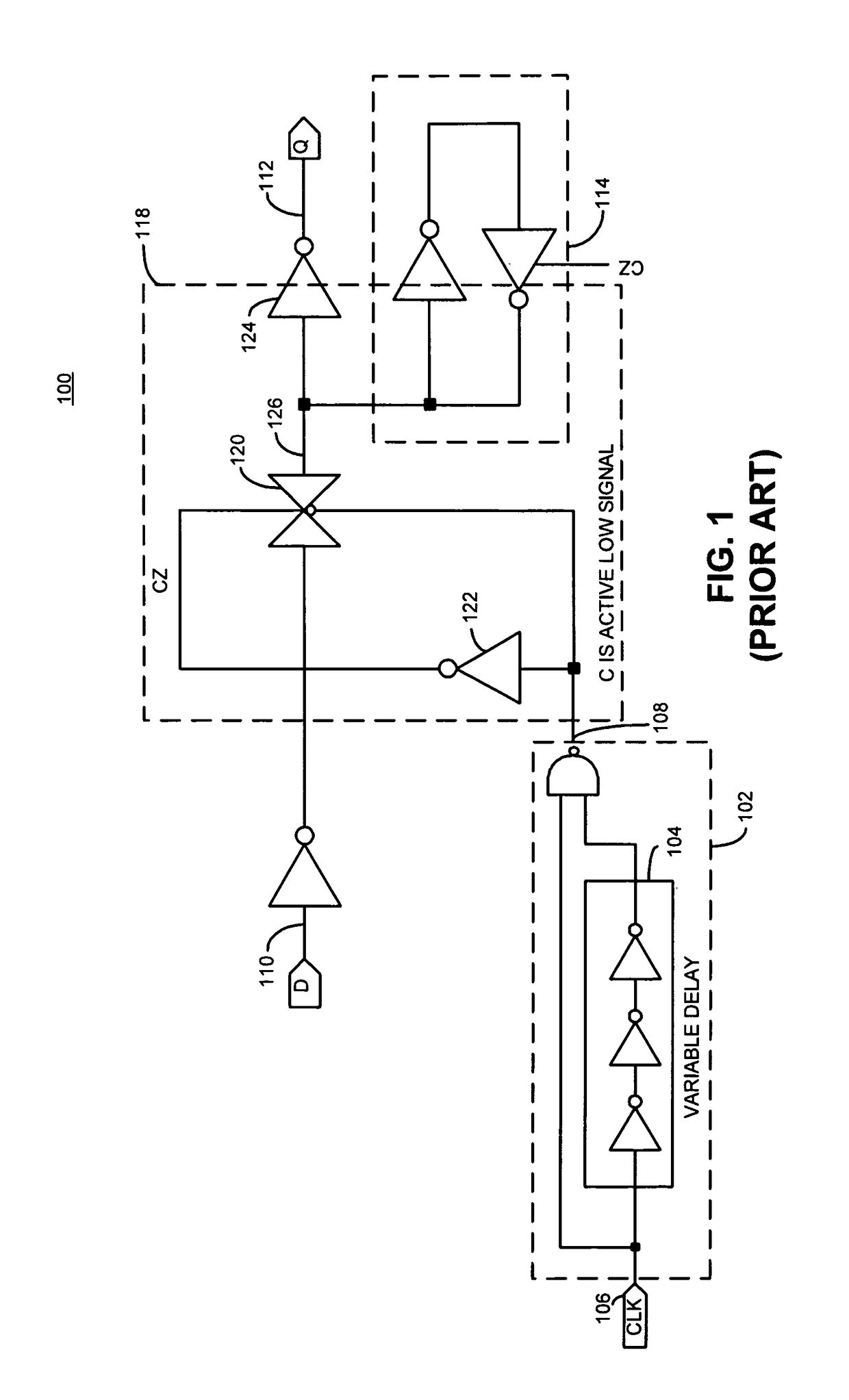
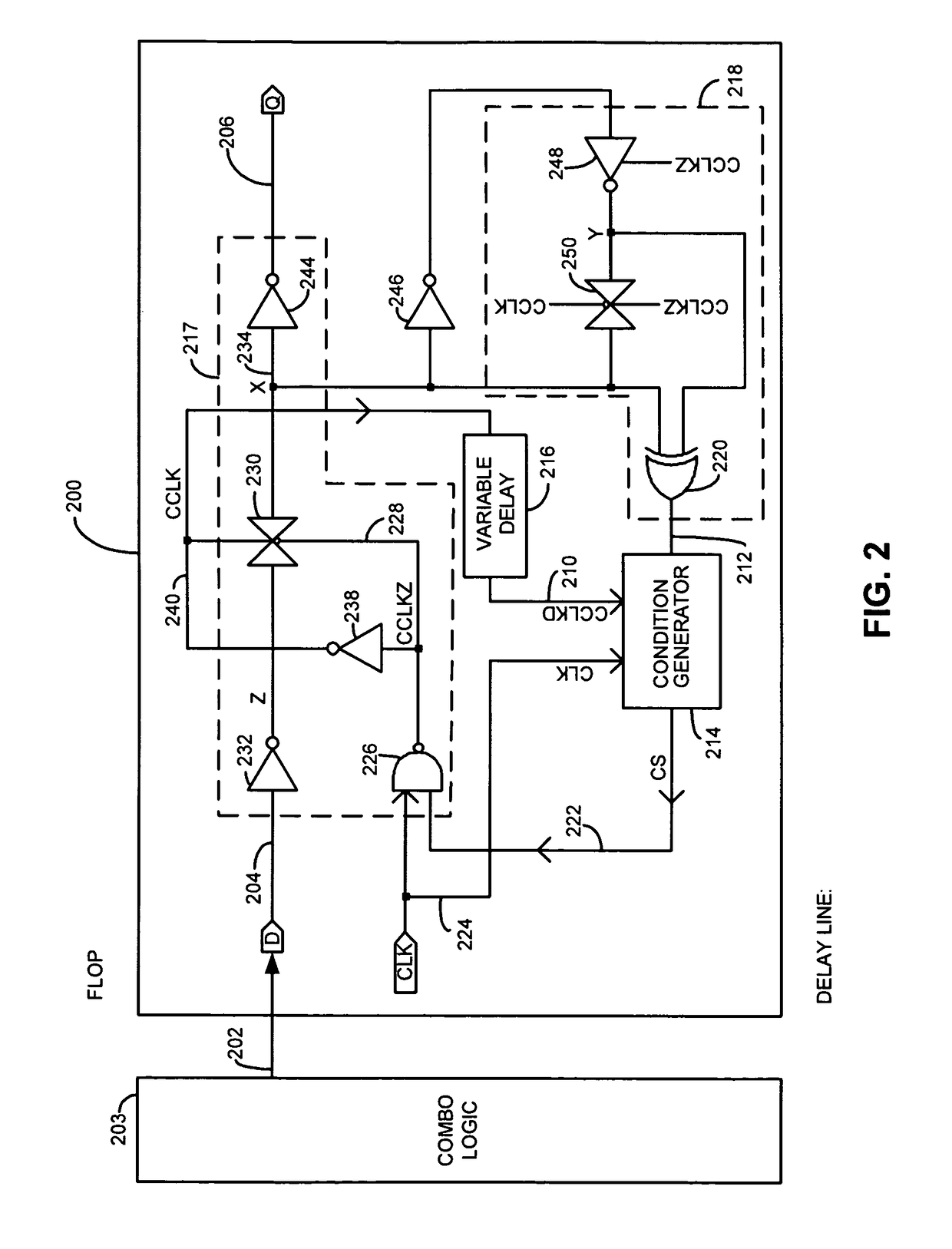
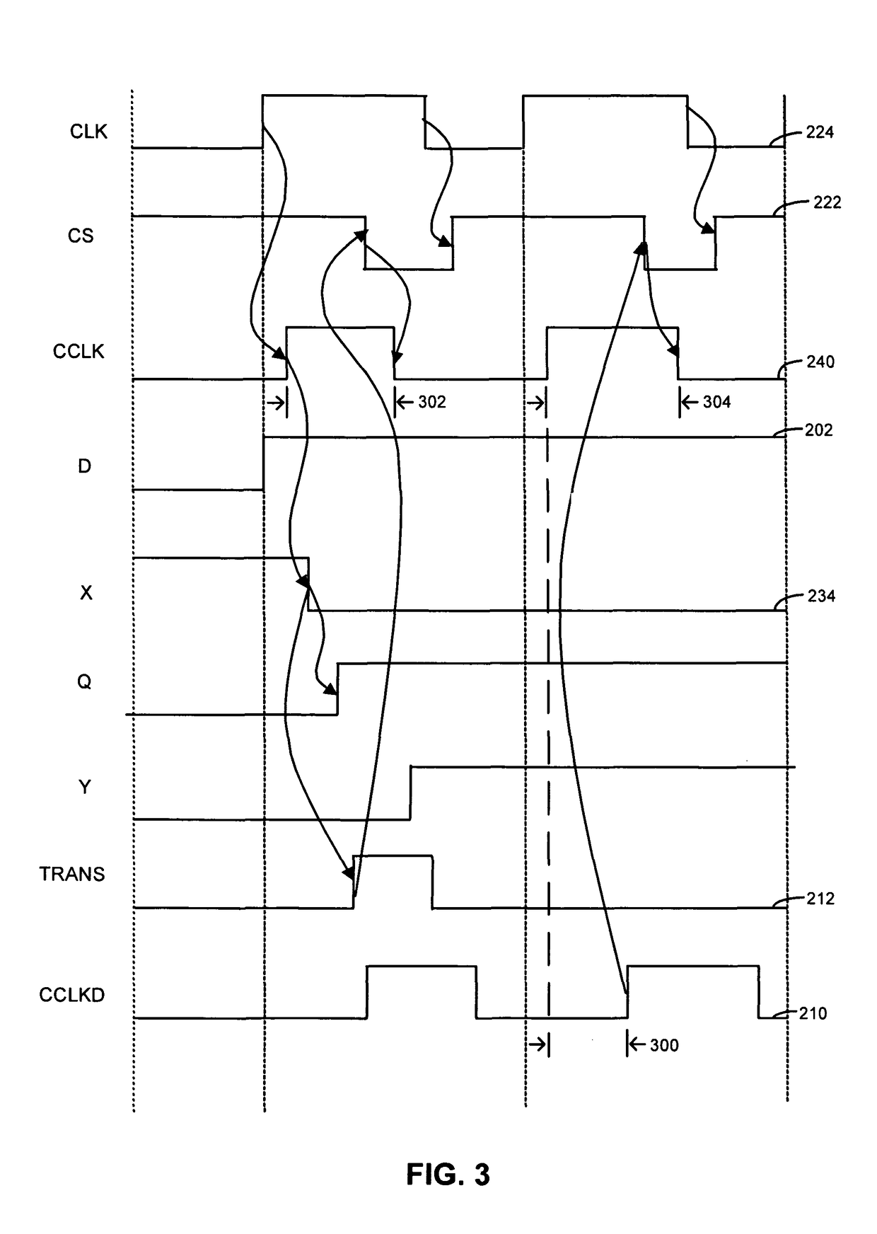
[0013]Generally, a pulsed latch circuit with conditional shutoff prevents an input node, such as a node receiving data, of the pulsed latch circuit, from latching data based on a delayed input control signal, such as an internal clocking signal, and based on a feedback latch state transition detection signal indicating that a current state of input data is stored in the latch. As such, two control conditions are used to shut down the latch. In one example, a condition generator detects when the latch has captured data correctly and outputs a signal to disable the input node. In addition, a variable delay circuit is used to adjust the width of the allowable input signal to set a worst case shutoff time. If data is latched early, a feedback latch state transition detection signal causes the input node to be disabled. If data is not latched early, the maximum allowable latch time is set by the variable delay circuit.

[0014]Stated another way, the condition generator logic disables the i...


PUM


Abstract

A pulsed latch circuit with conditional shutoff prevents an input node, such as a node receiving data, of the pulsed latch circuit, from latching data based on a delayed input control signal, such as an internal clocking signal, and based on a feedback latch state transition detection signal indicating that a current state of input data is stored in the latch. As such, two control conditions are used to shut down the latch. In one example, a condition generator detects when the latch has captured data correctly and outputs a signal to disable the input node. In addition, a variable delay circuit is used to adjust the width of the allowable input signal to set a worst case shutoff time. If data is latched early, a feedback latch state transition detection signal causes the input node to be disabled. If data is not latched early, the maximum allowable latch time is set by the variable delay circuit.

Description

BACKGROUND OF THE INVENTION[0001]The invention generally relates to integrated circuits that employ latches or flip-flops, and more particularly to pulsed latch circuits.[0002]Integrated circuits such as microprocessors and other integrated circuits employ combinational logic whose output is latched by flip-flops or latch circuits. The output of a latch circuit then serves as input to other combination logic and so on. In high performance chip designs, it is important for such synchronous designs to minimize the sequential overhead amongst the delays in the combinational logic and the flip-flops. The clock period to the flip-flops is increasingly becoming shorter and shorter to increase the speed of operation of the integrated circuit. As the combinational logic is getting more complex and the latch circuits between them operate on smaller clock pulses, process variations from the manufacturing process, which can increase or vary the hold time required for a latch to latch the incom...

Claims


Application Information

Patent Timeline
Patent Type & Authority Patents(United States)
IPC IPC(8): H03K3/356H03K3/037
CPCH03K3/0375H03K3/356156
Inventor IYER, ARUNPATEL, SHIBASHISHJAIN, ANIMESH
Owner ATI TECH INC
Why Eureka
Try Eureka