Local bottom gates for graphene and carbon nanotube devices

a carbon nanotube and graphene technology, applied in the direction of nanotechnology, semiconductor devices, electrical equipment, etc., can solve the problems of scaling either of these nanomaterials, difficult to establish thin, uniform and high-quality dielectrics on their surfaces, and nearly impossible to nucleate or deposit insulators

Active Publication Date: 2012-02-28
GLOBALFOUNDRIES U S INC
View PDF12 Cites 34 Cited by
  • Summary
  • Abstract
  • Description
  • Claims
  • Application Information

AI Technical Summary

Problems solved by technology

One of the foremost challenges to scaling either of these nanomaterials is the difficulty of establishing thin, uniform and high-quality dielectrics on their surfaces.
The absence of open surface bonds makes it nearly impossible to nucleate or deposit insulators, especially with the monolayer accuracy that is needed for scaled gate dielectrics.
However, the molecular layers have been shown to interact with the carbon bonds, creating scattering centers that cause the mobility to suffer greatly.
In fact, since all carriers are on the surface of these nanostructures the carriers strongly couple to any material that is deposited around them, causing degradation of the transport properties.
Additionally, when using molecules such as deoxyribonucleic acid (DNA) to create a nucleation layer around carbon nanotubes the uniformity can be compromised as a result of the relatively large molecule diameter (four nm for DNA) compared to the carbon nanotubes (about 1.5 nm).

Method used


Image

  • Local bottom gates for graphene and carbon nanotube devices
  • Local bottom gates for graphene and carbon nanotube devices
  • Local bottom gates for graphene and carbon nanotube devices

Examples


Embodiment Construction

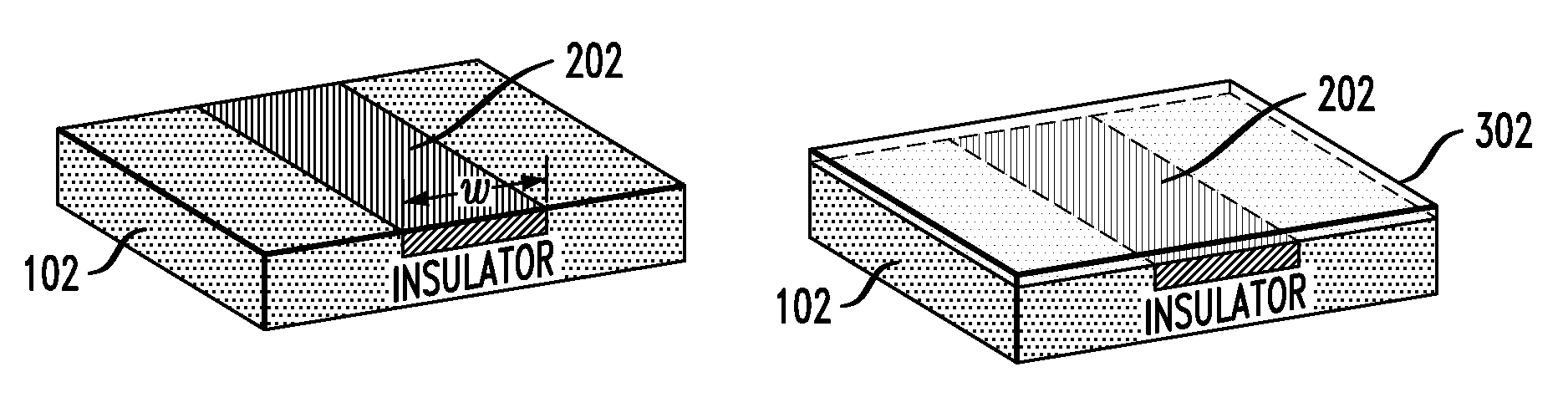
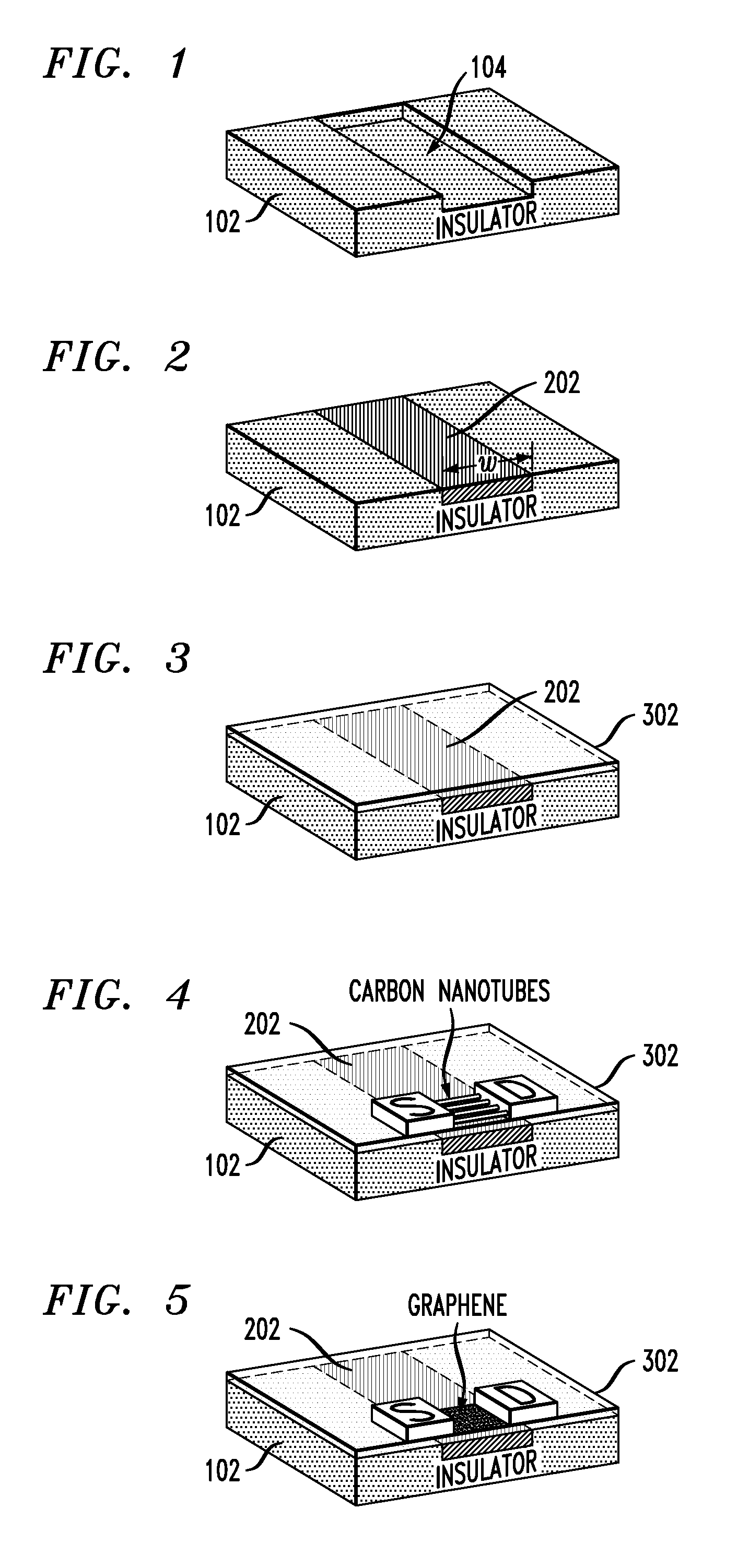
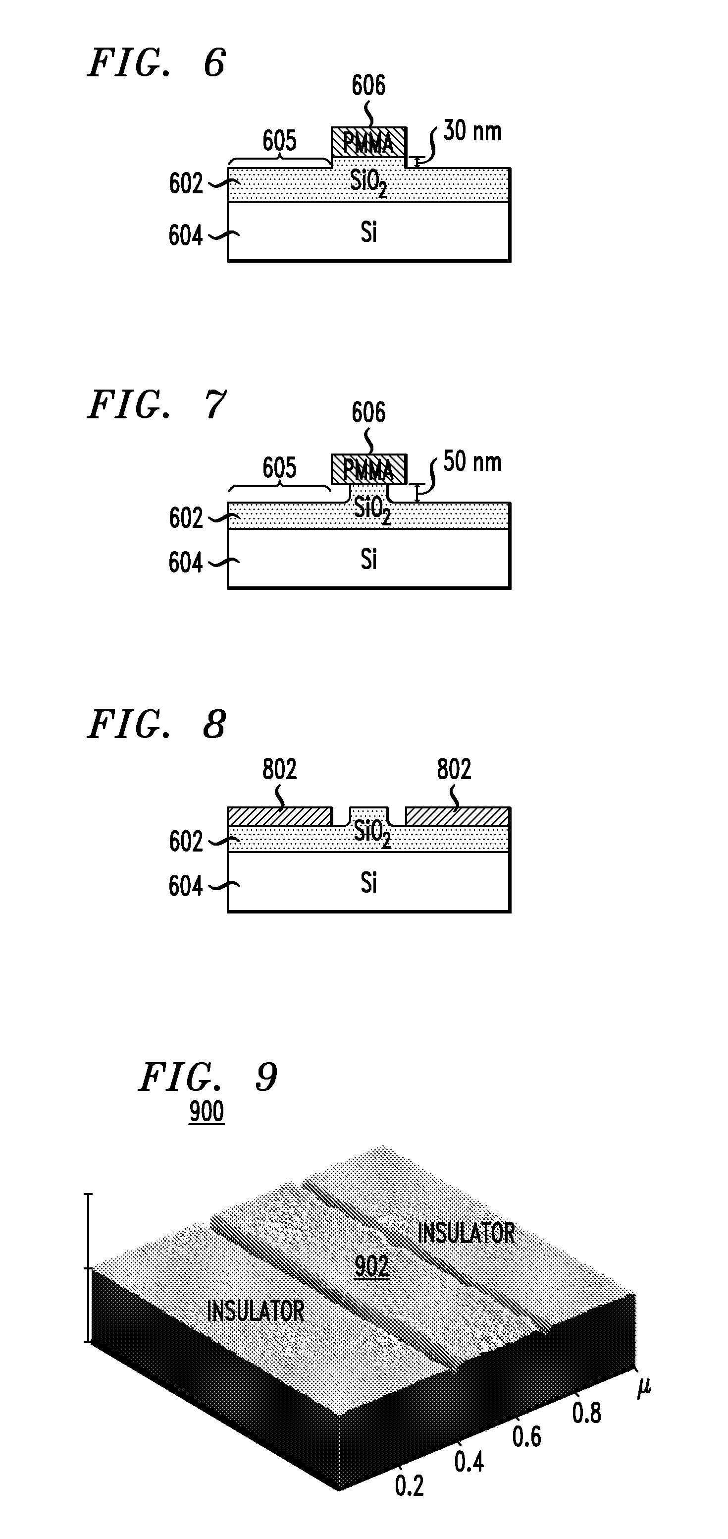
[0022]FIGS. 1-5 are diagrams illustrating an exemplary methodology for fabricating a transistor device having a channel formed from a nanoscale material, such as carbon nanotubes or graphene. In general, a transistor includes a source and a drain connected by a channel(s), and a gate which regulates electron flow through the channel. The gate is separated from the channel by a dielectric material (a gate dielectric). As will be described in detail below, the present process flow involves forming a local bottom gate and ultra-thin gate dielectric prior to placing the channel over the dielectric, which avoids altogether the above-described problems associated with trying to form the dielectric on the carbon nanotube / graphene material (in this manner, the dielectric thickness and uniformity are entirely independent of the channel material used allowing the device to be scaled aggressively). To do so, the gate needs to be flush with a surrounding insulator, allowing for the channel mate...


PUM

PropertyMeasurementUnit
thicknessaaaaaaaaaa
diameteraaaaaaaaaa
thicknessaaaaaaaaaa

Abstract

Transistor devices having nanoscale material-based channels and techniques for the fabrication thereof are provided. In one aspect, a transistor device includes a substrate; an insulator on the substrate; a gate embedded in the insulator with a top surface of the gate being substantially coplanar with a surface of the insulator; a dielectric layer over the gate and insulator; a channel comprising a carbon nanostructure material formed on the dielectric layer over the gate, wherein the dielectric layer over the gate and the insulator provides a flat surface on which the channel is formed; and source and drain contacts connected by the channel. A method of fabricating a transistor device is also provided.

Description

STATEMENT OF GOVERNMENT RIGHTS[0001]This invention was made with Government support under Contract number FA8650-08-C-7838 awarded by (DARPA) Defense Advanced Research Projects Agency. The Government has certain rights in this invention.FIELD OF THE INVENTION[0002]The present invention relates to transistor devices, and more particularly, to transistor devices having nanoscale material-based channels (e.g., carbon nanotube or graphene channels) and techniques for the fabrication thereof.BACKGROUND OF THE INVENTION[0003]The integration of carbon nanostructures as channel materials in the next generation of electronic devices offers many advantages over the continued scaling of silicon (Si). Carbon nanotubes and graphene are two nanoscale forms of carbon that exhibit extremely high current carrying capacity and mobilities several orders of magnitude beyond the theoretical limit for Si. Additionally, carbon nanotubes (one-dimensional) and graphene (two-dimensional) are low-dimensional ...

Claims


Application Information

Patent Timeline
Patent Type & Authority Patents(United States)
IPC IPC(8): H01L21/00H01L21/84
CPCB82Y10/00H01L29/1606H01L29/7781H01L29/78684H01L51/0525H01L51/0545H01L51/0048H01L51/0516H01L51/055H10K85/221H10K10/468H10K10/472H10K10/481H10K10/466
Inventor CHEN, ZHIHONGFRANKLIN, AARON D.HANNON, JAMES B.TULEVSKI, GEORGE S.
Owner GLOBALFOUNDRIES U S INC
Why Eureka
Try Eureka