Chip package solder interconnect formed by surface tension

a surface tension and interconnection technology, applied in the field of integrated circuit (ic) chip package processing, can solve problems such as failure of chip, solder, connection, etc., and achieve the effect of facilitating chip joining

Inactive Publication Date: 2012-03-20
GLOBALFOUNDRIES INC
View PDF2 Cites 6 Cited by
  • Summary
  • Abstract
  • Description
  • Claims
  • Application Information

AI Technical Summary

Benefits of technology

[0006]A second aspect of the disclosure provides a solder self-assembly structure for an IC chip comprising: a release layer disposed on a portion of an upper surface of the substrate, laterally spaced from a via in the substrate; a barrier layer metallization (BLM) disposed in a first part over a portion of the substrate including a via, and in a second part over th

Problems solved by technology

The increasing demand for smaller solder bumps, higher current per bump, larger die sizes, and other features drive increasingly challenging requirements for bump electrical, thermal, and mechanical performance, particularly with flip chip plastic ball grid array organic laminate packages

Method used


Image

  • Chip package solder interconnect formed by surface tension
  • Chip package solder interconnect formed by surface tension
  • Chip package solder interconnect formed by surface tension

Examples


Embodiment Construction

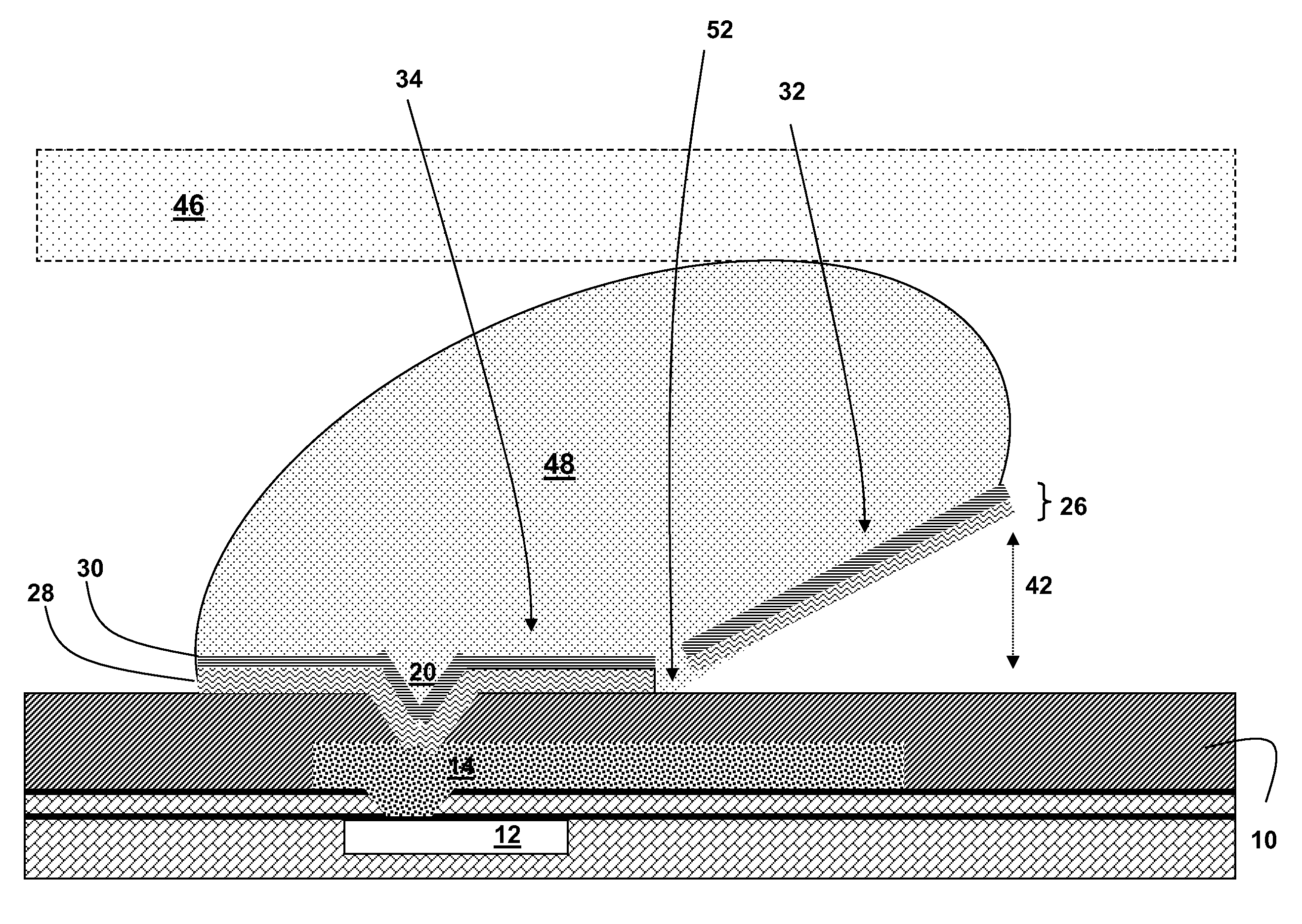
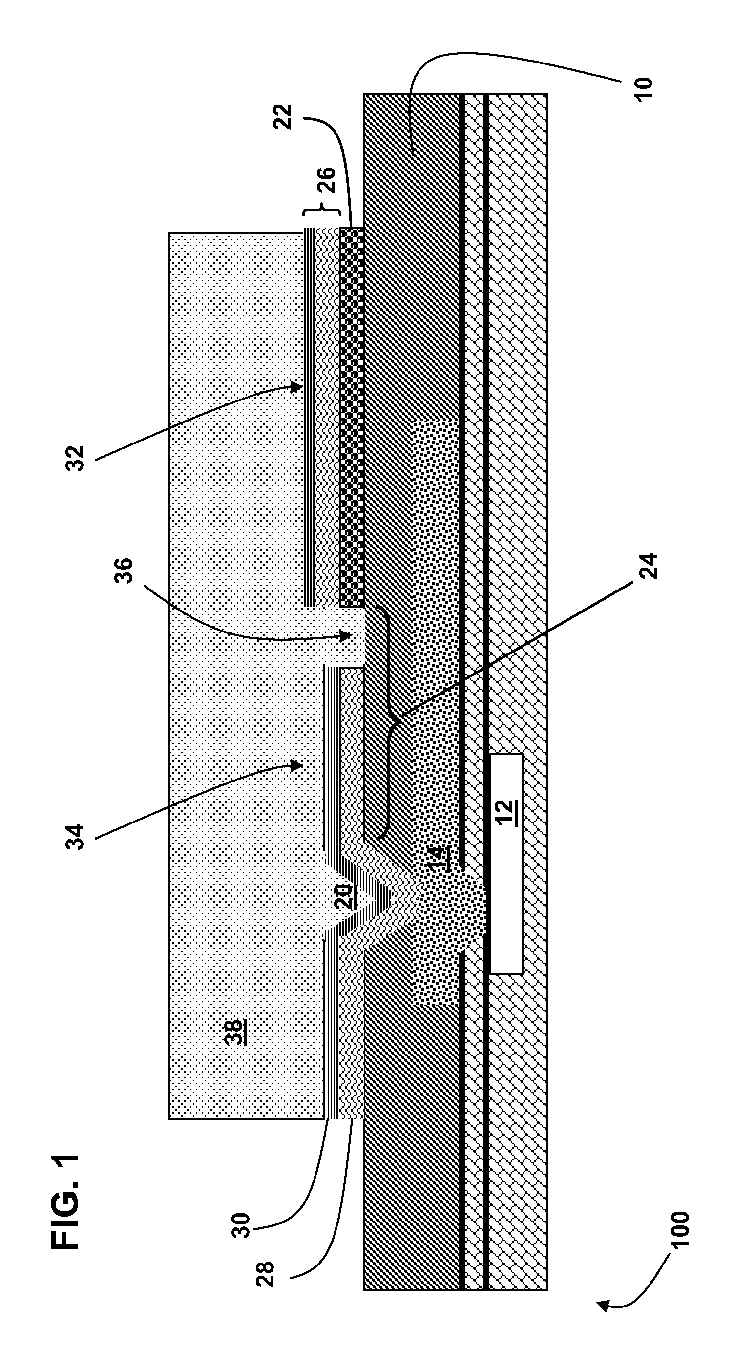
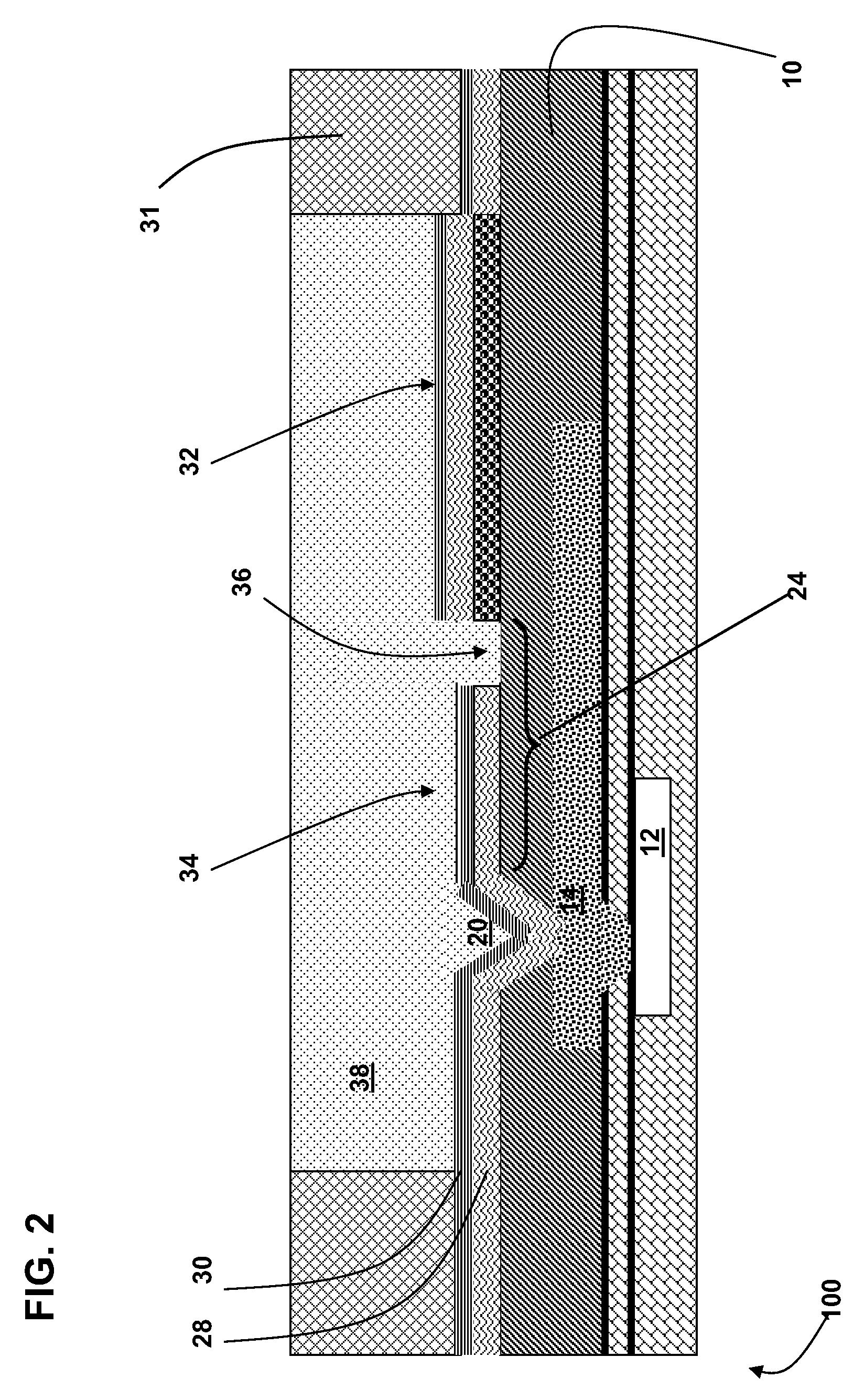
[0017]Referring to the drawings, FIGS. 1-6 depict a solder structure for an integrated circuit (IC) chip package and method of making the same in accordance with embodiments of the invention.

[0018]FIGS. 1-2 shows a substrate 10, which may be polyimide, and which may include copper wire 12, aluminum pad 14, and other features as known in the art. Via 20 may be etched in substrate 10. A release layer is deposited over a portion of a surface of substrate 10 and patterned, forming release layer 22 laterally distanced from via 20 by a first distance 24. In one embodiment, release layer 22 may comprise SiO2. In other embodiments, release layer 22 may be Si, Ge, Al, Ti, W, a polymer, or SiN.

[0019]As shown in FIGS. 1-2, a barrier layer metallization (BLM) 26 is deposited over a surface of substrate 10 and release layer 22. BLM 26 includes a first layer 28 over release layer 22 and substrate 10, and a second layer 30 over first layer 28. In various embodiments, first layer 28 of BLM 26 may c...


PUM


Abstract

Disclosed herein is a solder self-assembly structure, an IC chip including a solder self-assembly structure, and a method of making the same. The structure includes a release layer disposed on a portion of an upper surface of the substrate, laterally spaced from a via in the substrate. A barrier layer metallization (BLM) is disposed in a first part over a portion of the substrate including a via, and in a second part over the release layer, leaving a surface of the substrate exposed between the first portion and the second portion of the BLM. A solder structure is disposed over the first and second portions of the BLM and the exposed surface of the substrate disposed there between. When the solder structure is reflowed and annealed, surface tension in the solder causes self-assembly of a three-dimensional, compliant solder structure.

Description

FIELD OF THE INVENTION[0001]This disclosure relates generally to integrated circuit (IC) chip package processing, and more particularly to the production of IC chip packages using a self-assembly controlled collapse chip connection (C4) solder structure formed using surface tension to join an IC chip to a package.BACKGROUND[0002]Lead-free (Pb-free) solder bumping technology is replacing the use of high-Pb alloys for chip package interconnection in advanced integrated circuit (IC) technologies. The increasing demand for smaller solder bumps, higher current per bump, larger die sizes, and other features drive increasingly challenging requirements for bump electrical, thermal, and mechanical performance, particularly with flip chip plastic ball grid array organic laminate packages.[0003]Standard processing methods may encounter challenges, however. Due to the coefficient of thermal expansion of the solder, following chip package join by reflowing and annealing the solder, the solder ma...

Claims


Application Information

Patent Timeline
IPC IPC(8): H01L21/302
CPCB81C1/00325H01L24/11H01L24/13H01L24/16H01L24/81H01L2224/05027H01L2224/13015H01L2224/14131H01L2224/05124H01L2224/05155H01L2224/05166H01L2224/05184H01L2224/05644H01L2224/05647H01L2224/05655H01L2224/05671H01L2224/05672H01L2224/11001H01L2224/11334H01L2224/11462H01L2224/1147H01L2224/13018H01L2224/141H01L2224/16057H01L2224/81002H01L2224/81143H01L2224/81815H01L2924/01327H01L2224/05572H01L2224/131H01L2224/16227H01L2924/00013H01L2924/01029H01L2224/05022H01L2224/05147H01L2224/05552H01L2224/06051H01L2224/13027H01L2224/16225H01L2224/0401H01L2924/00014H01L2924/01074H01L2924/01023H01L2924/00012H01L2224/13099H01L2224/13599H01L2224/05599H01L2224/05099H01L2224/29099H01L2224/29599H01L2924/014H01L2924/14H01L2924/00
Inventor DAUBENSPECK, TIMOTHY H.GAMBINO, JEFFREY P.MUZZY, CHRISTOPHER D.SAUTER, WOLFGANGSULLIVAN, TIMOTHY D.
Owner GLOBALFOUNDRIES INC
Why Eureka
Try Eureka