Solid-state image sensor

a solid-state image and sensor technology, applied in the field of solid-state image sensors, can solve the problem of unintentional incident light upon the pixel, and achieve the effect of suppressing color mixture and suppressing the increase of load capacitance of transfer gates

Active Publication Date: 2012-04-03
SEMICON COMPONENTS IND LLC
View PDF3 Cites 0 Cited by
  • Summary
  • Abstract
  • Description
  • Claims
  • Application Information

AI Technical Summary

Benefits of technology

[0009]The present invention has been proposed in order to solve the aforementioned problem, and an object of the present invention is to provide a solid-state image sensor capable of suppressing color mixture while suppressing increase of load capacitances of transfer gates and a short circuit between two adjacent transfer gates.

Problems solved by technology

In this case, color mixture disadvantageously results from the incidence of the unintentional incident light upon the pixel 101 adjacent to the prescribed pixel 101.

Method used


Image

  • Solid-state image sensor
  • Solid-state image sensor
  • Solid-state image sensor

Examples


first embodiment

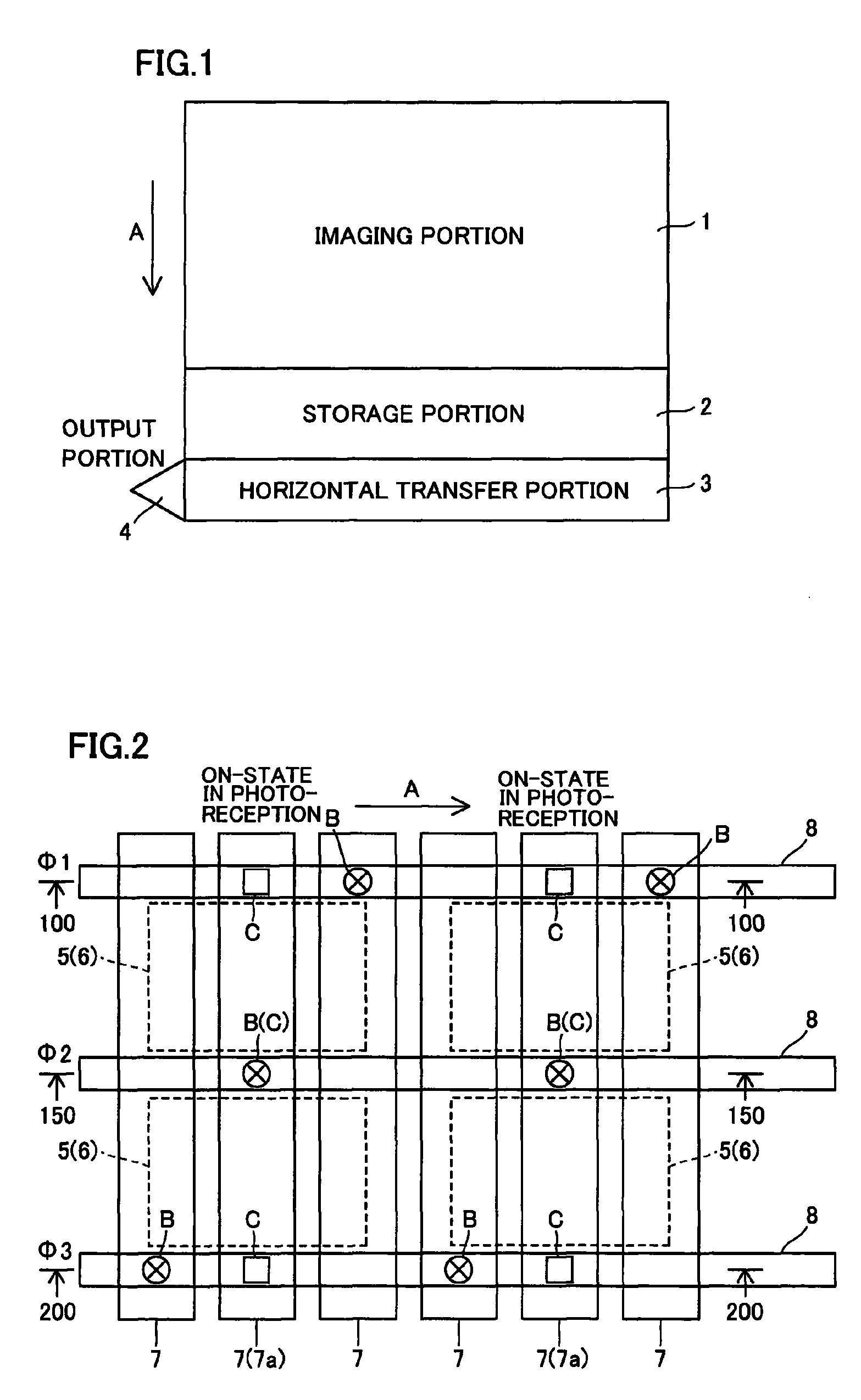
[0050]Referring to FIGS. 1 to 5, a first embodiment of the present invention is applied to a frame transfer solid-state image sensor.

[0051]As shown in FIG. 1, the frame transfer solid-state image sensor according to the first embodiment comprises an imaging portion 1, a storage portion 2, a horizontal transfer portion 3 and an output portion 4. The imaging portion 1 is provided for performing photoelectric conversion by incidence of light. A plurality of pixels 5 are arranged on the imaging portion 1 in the form of a matrix, as shown in FIG. 2. Photoelectric conversion portions 6 are provided on regions corresponding to the pixels 5 respectively. The imaging portion 1 has a function of storing generated electrons (charge) and transferring the same to the storage portion 2. The storage portion 2 has a function of storing the electrons received from the imaging portion 1 and transferring the same to the horizontal transfer portion 3 (see FIG. 1). The horizontal transfer portion 3 has ...

second embodiment

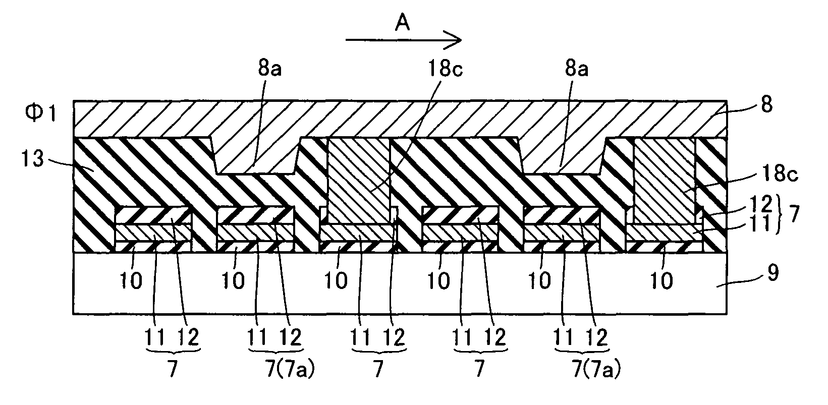
[0067]Referring to FIGS. 6 to 8, shielding material lines 8 are connected to corresponding transfer gates 7 through transparent plugs 18c (18d) of polysilicon in an imaging portion of a solid-state image sensor according to a second embodiment of the present invention, dissimilarly to the aforementioned first embodiment. The plugs 18c (18d) are examples of the “connecting portion” in the present invention.

[0068]More specifically, the shielding material line 8 transmitting a clock signal Φ1 and the transfer gates 7 adjacent to transfer gates 7a entering ON-states in photoreception along an electron transfer direction (along arrow A) are connected with each other through the corresponding plugs 18c according to the second embodiment, as shown in FIG. 6. As shown in FIG. 8, further, the shielding material line 8 transmitting a clock signal Φ3 and the transfer gates 7 adjacent to the transfer gates 7a entering ON-states in photoreception oppositely to the electron transfer direction (al...

third embodiment

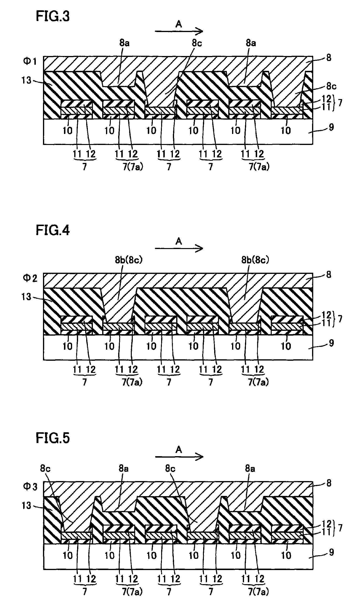
[0071]Referring to FIG. 9, projecting portions 8b (see FIG. 7) provided on a shielding material line 8 transmitting a clock signal Φ2 are directly connected to transfer gates 7a entering ON-states in photoreception to function also as connecting portions 8c in an imaging portion of a solid-state image sensor according to a third embodiment of the present invention, dissimilarly to the aforementioned second embodiment shown in FIGS. 6 to 8. More specifically, the projecting portions 8b projecting downward from the lower surface of the shielding material line 8 transmitting the clock signal Φ2 are formed to reach polysilicon films 11 through SiN films 12 of the corresponding transfer gates 7a. The projecting portions 8b project downward by about 450 nm from the lower surface of the shielding material line 8.

[0072]According to the third embodiment, the projecting portions 8b are formed to be reduced in width as approaching to the transfer gates 7a. The width of parts of the projecting ...


PUM


Abstract

A solid-state image sensor capable of suppressing color mixture while suppressing increase of load capacitances of transfer gates and a short circuit between two adjacent transfer gates is provided. This solid-state image sensor comprises a plurality of transfer gates and a shielding material line blocking light incident from above a prescribed pixel upon another pixel adjacent to the prescribed pixel. The shielding material line has a downward projecting portion on a region corresponding to at least one transfer gate entering an ON-state in photoreception.

Description

BACKGROUND OF THE INVENTION[0001]1. Field of the Invention[0002]The present invention relates to a solid-state image sensor, and more particularly, it relates to a solid-state image sensor comprising a shielding material line for blocking light incident from above a prescribed pixel upon another pixel adjacent to the prescribed pixel.[0003]2. Description of the Background Art[0004]Various solid-state image sensors each comprising a shielding material line for blocking light incident from above a prescribed pixel upon another pixel adjacent to the prescribed pixel are known in general. Such a solid-state image sensor is disclosed in ITE Technical Report Vol. 28, No. 25, pp. 13-16, IST2004-25 (May, 2004), for example.[0005]FIG. 16 is a plan view showing the structure of an imaging portion of an exemplary conventional solid-state image sensor comprising shielding material lines. FIG. 17 is a sectional view of the imaging portion of the exemplary conventional solid-state image sensor ta...

Claims


Application Information

Patent Timeline
Patent Type & Authority Patents(United States)
IPC IPC(8): H03F1/32H01L27/14H04N5/335H04N5/357H04N5/369H04N5/3725
CPCH01L27/14623H01L27/14812H01L27/1485H01L31/02162
Inventor ICHIHASHI, YOSHINARISHIMIZU, RYUSASADA, KAZUHIRO
Owner SEMICON COMPONENTS IND LLC
Why Eureka
Try Eureka