Compact high-speed modulator driver method and apparatus

a high-speed modulator and driver technology, applied in the field of digital communication devices, can solve the problems of difficult adjustment of output signal amplitude and duty cycle, several limitations of modulator driver use, and difficult to achieve large-amplitude drive signal at high-speed data rate, so as to reduce the number of components and transitions

Inactive Publication Date: 2012-04-03
KITEL TECH
View PDF16 Cites 8 Cited by
  • Summary
  • Abstract
  • Description
  • Claims
  • Application Information

AI Technical Summary

Benefits of technology

[0008]Modulator driver for driving an electro-optical modulator in a high-speed optical communications system. In accordance with aspects of the present invention, a modulator driver is presented comprising an input differential limiting amplifier which is coupled to a distributed differential switch configuration, where one set of outputs of the distributed differential switch configuration are grounded and the other set of outputs are connected to an artificial transmission line structure generating forward traveling and reverse traveling signals, with the reverse traveling signal termination bias inductively coupled to a separately adjustable positive bias voltage, whereby the circuit architecture reduces the number of components and transitions in the high-speed signal path and is compatible with compact, monolithic fabrication requiring a minimal amount of external components for operation. Other methods and apparatus are presented.

Problems solved by technology

A large amplitude drive signal is difficult to achieve at high-speed data rates due to the parasitics of the transistor device sizes required to generate the large electrical output voltage swings.
While the topology in FIG. 2 can provide wideband amplification and large output amplitude capability, it has several limitations when used for modulator driver applications.
One limitation is that adjustment of the output signal amplitude and duty cycle can be difficult, typically requiring external circuitry for simultaneous adjustment of the supply voltage VCC and gate bias voltage VG.
Another limitation is that the gain of this distributed amplifier topology is typically lower than required for single-ended modulator driver applications.
A further limitation is that stabilization of the output signal amplitude over a range of input signal amplitudes can be difficult, typically requiring amplifier saturation which can cause poorly controlled output signal rise and fall times. Finally, typical inter-stage bias-T components for the broadband transmission of data are inconsistent with monolithic IC fabrication techniques, which can result in the use of bulky multi-chip modules to achieve the modulator driver function.

Method used


Image

  • Compact high-speed modulator driver method and apparatus
  • Compact high-speed modulator driver method and apparatus
  • Compact high-speed modulator driver method and apparatus

Examples


Embodiment Construction

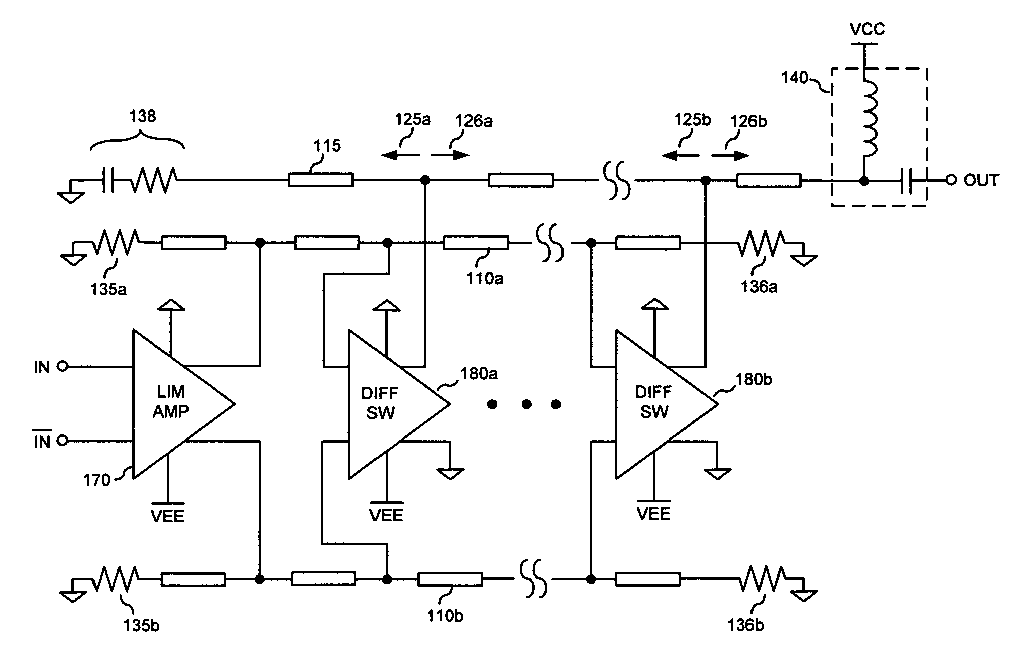
[0019]A modulator driver arrangement is presented in FIG. 4 as one embodiment of aspects of the present invention. In this arrangement, an input signal is coupled to a limiting amplifier 170 which provides an input signal limiting function and outputs a differential output signal with a leveled amplitude. The limiting amplifier has the ability to accept differential input signals as illustrated in FIG. 4, or a single-ended input signal coupled to one input of the limiting amplifier 170 through a DC blocking capacitor, with the limiting amplifier 170 further providing a single-ended to differential signal conversion function. The output differential signal from limiting amplifier 170 is coupled to a differential artificial transmission line comprised of inductive elements 110a, 110b disposed between differential signal inputs to differential current switches 180a, 180b, and further comprised of reverse differential traveling wave signal termination resistors 135a, 135b as well as for...


PUM


Abstract

Modulator driver for driving an electro-optical modulator in a high-speed optical communications system. In accordance with aspects of the present invention, a modulator driver is presented comprising an input differential limiting amplifier which is coupled to a distributed differential current-switch configuration, where one set of outputs of the distributed differential current-switch configuration are grounded and the other set of outputs are connected to an artificial transmission line structure generating forward traveling and reverse traveling signals, with the reverse traveling signal termination bias inductively coupled to a separately adjustable positive bias voltage, whereby the circuit architecture reduces the number of components and transitions in the high-speed signal path and is compatible with compact, monolithic fabrication requiring a minimal amount of external components for operation. Other methods and apparatus are presented.

Description

CROSS-REFERENCE TO RELATED APPLICATIONS[0001]This application claims the benefit of U.S. Provisional Application No. 61 / 072,503, filed Mar. 31, 2008 by the present inventor, which is incorporated herein by reference.FIELD OF THE INVENTION[0002]The subject matter disclosed generally relates to the field of digital communications devices. More specifically, the subject matter disclosed relates to electronic arrangements for high-speed, electro-optical data transmission applications.BACKGROUND OF THE INVENTION[0003]An important element in high-speed fiber-optic transmission systems is the ability to optically encode data bits for transport in optical fiber media. One way this is achieved is through the modulation of the output of a continuous-wave laser source by an electro-optical modulator, whose output is coupled to an optical fiber for transmission. Many applications require high quality optical modulation performance, which imposes amplitude and signal quality requirements on the ...

Claims


Application Information

Patent Timeline
Patent Type & Authority Patents(United States)
IPC IPC(8): H04B10/04
CPCH03F3/45089H03F3/45475H03F3/602H03F3/607H03F2203/45136H03F2203/45612G02F1/0327
Inventor BONTHRON, ANDREW JOHN
Owner KITEL TECH
Why Eureka
Try Eureka