Check patentability & draft patents in minutes with Patsnap Eureka AI!

Method of manufacturing multi-touch liquid crystal display panel

a liquid crystal display and multi-touch technology, applied in the direction of liquid surface applicators, instruments, coatings, etc., can solve the problems of easy cracking of easy cracking of the climb breaking and cracking of the ito electrode layer, and increase the thickness and weight of the touch panel due to the attached device, so as to achieve a simple and low cost manufacturing process, prevent the cracking of the climb breaking and the effect of increasing the thickness and weight of the multi-touch

Active Publication Date: 2012-06-12
CENTURY DISPLAY (SHENZHEN) CO LTD
View PDF4 Cites 0 Cited by
  • Summary
  • Abstract
  • Description
  • Claims
  • Application Information

AI Technical Summary

Benefits of technology

[0009]In view of the above problems, the main objective of the present invention is to provide a method of manufacturing a multi-touch LCD panel which resolves the above problems such as climb breaking and cracking of the ITO electrode layer. By forming the touch sensing layer within the liquid crystal cell, the thickness and weight of the multi-touch LCD panel can be significantly streamlined, so as to meet the “small & light” requirements of current electrical products. Moreover, it would be relatively simple, low-cost, and capable of preventing the ITO electrode layer from experiencing the climb breaking and cracking phenomena. By introducing a process of forming the touch sensing layer after the conventional color filter manufacturing process, the aforesaid shortcomings are resolved and the product yield is improved as well.
[0012]The method of manufacturing a multi-touch LCD panel provided in the present invention includes forming the touch sensing layer within the liquid crystal cell instead of attaching another touch sensing device onto the display panel as shown in the conventional arts. The thickness and weight of the multi-touch LCD panel can therefore be streamlined and the “short & light” requirements of current electrical products can be satisfied. Furthermore, the present invention does not need to change the conventional color filter substrate manufacturing method, but still reaps the benefits of providing a simple and low cost manufacturing process by attaching the conductive colloidal mixture onto appropriate locations of the electrode layer while the color filter substrate is provided with the electrode layer being already formed thereon. Meanwhile, by forming the conductive particles on the electrode layer instead of forming the electrode layer on the protrusion as in the prior art, the present invention does not need to form the protrusion, so that the drawbacks of climb breaking and cracking of the ITO electrode layer will be prevented. The product yield can therefore be improved as well.

Problems solved by technology

The aforementioned manufacturing methods require attaching the touch sensing device onto the display panel, and therefore the thickness and weight of the touch panel will increase due to the attached device.
According to the manufacturing process of the color filter substrate 220 (in sequence of forming a black matrix, a color filter layer, an ITO electrode layer, and a liquid crystal spacer), the drawbacks of climb breaking and cracking of the ITO electrode layer are prone to occur due to the protrusion's taper angle and height.

Method used


Image

  • Method of manufacturing multi-touch liquid crystal display panel
  • Method of manufacturing multi-touch liquid crystal display panel
  • Method of manufacturing multi-touch liquid crystal display panel

Examples


Embodiment Construction

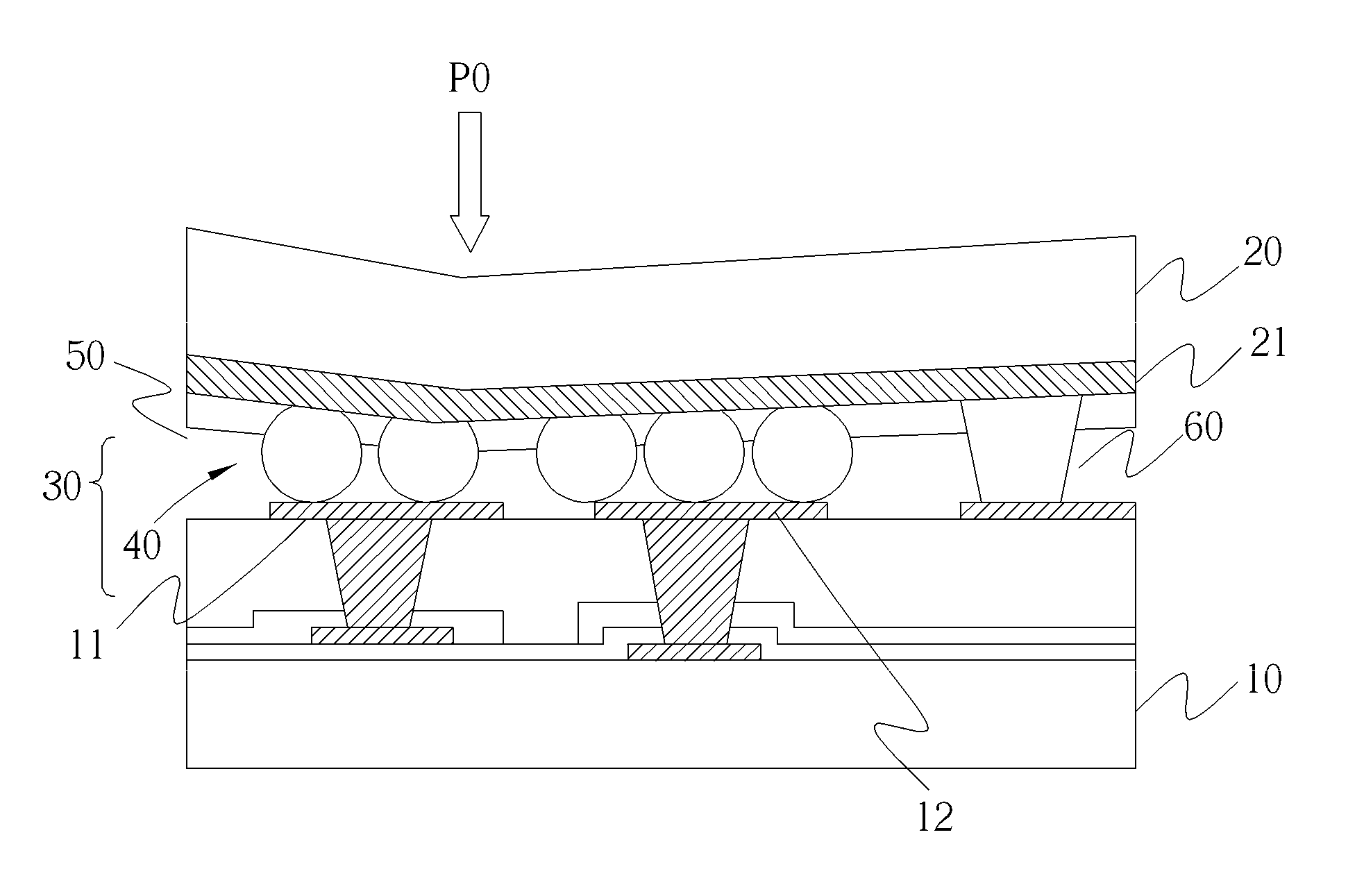
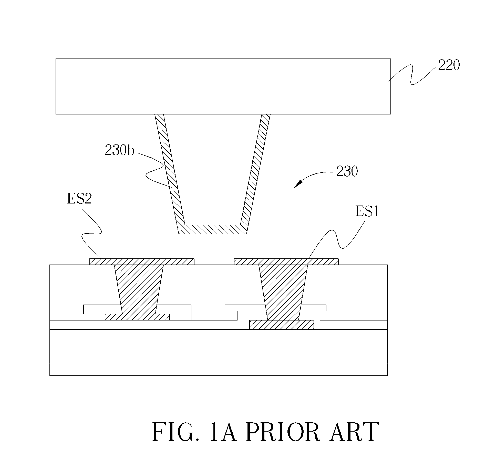
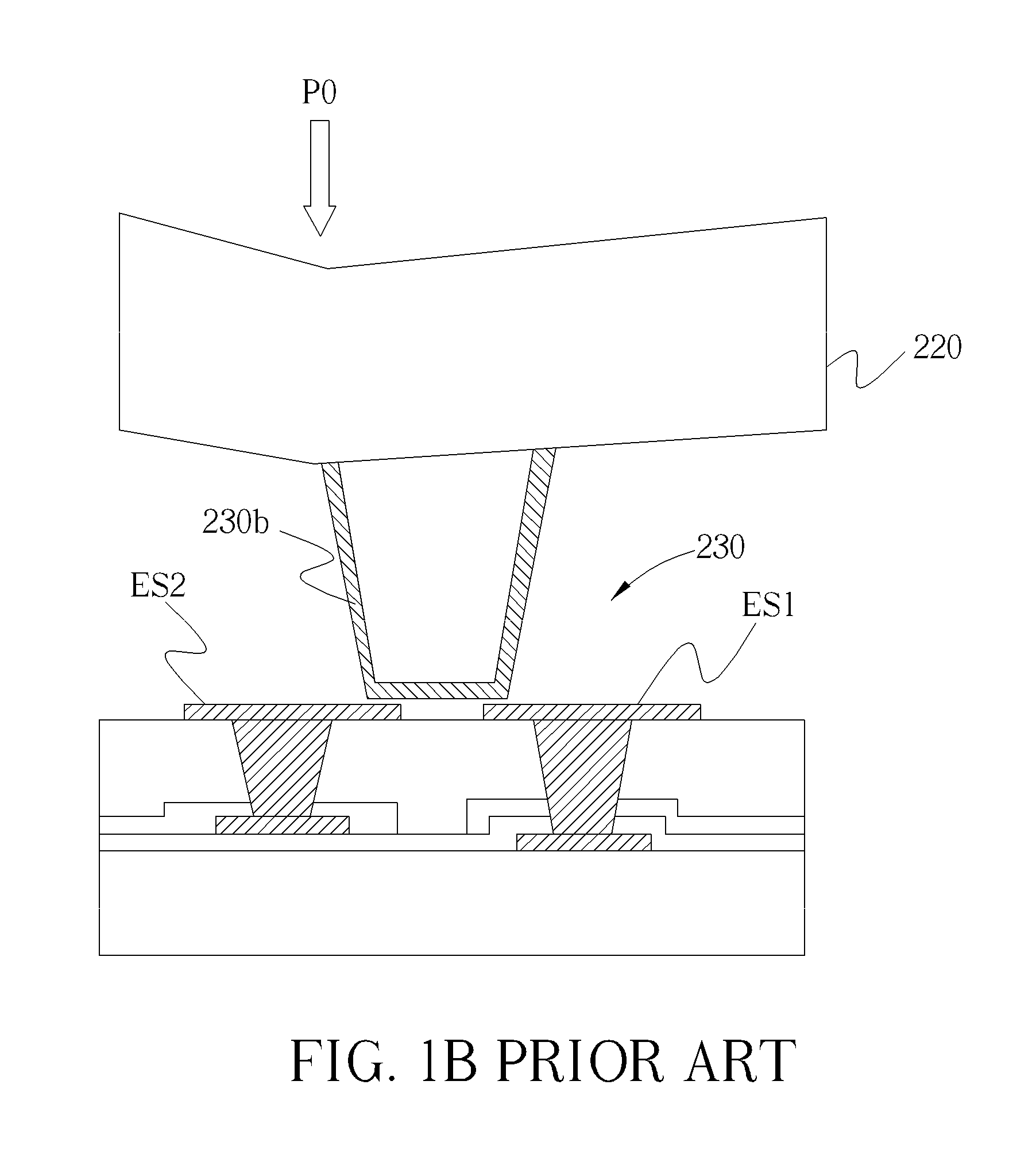
[0019]The numerals of the FIGs. in the present invention are shown as following:[0020]10 TFT array substrate[0021]11 first sensing electrode[0022]12 second sensing electrode[0023]20 color filter substrate[0024]21 electrode layer[0025]30 liquid crystal layer[0026]40 conductive particles[0027]50 Colloid[0028]60 liquid crystal spacer[0029]220 color filter substrate[0030]230 touch connecting component[0031]230b conductive layer[0032]ES1, ES2 touch sensing component[0033]Po external force

[0034]To provide a better understanding of the objective, the feature and the function of presented invention, detailed descriptions are shown as follows with reference to the accompanying drawings.

[0035]In order to describe the present invention with facility, the following preferred embodiment takes the manufacturing method of a TFT LCD panel as example, but should not be limited thereto in practice.

[0036]Please refer to FIG. 2, illustrating a flow chart of one embodiment of the method of manufacturing...


PUM

PropertyMeasurementUnit
transparentaaaaaaaaaa
conductiveaaaaaaaaaa
heightaaaaaaaaaa

Abstract

A method of manufacturing a multi-touch LCD panel. A conductive colloidal mixture formed by mixing a plurality of conductive particles and a colloid is coated on the electrode layer of the counter substrate and is solidified to make the conductive particles electrically connect to the corresponding sensing electrodes of the array substrate. Consequently, when an external force is applied to one touching position on the counter substrate, the conductive particles electrically connect the sensing electrodes to the electrode layer and the touching signal of the position can be obtained. Due to the integration of the conductive particles into the liquid crystal cell gap, the multi-touch LCD panel has the advantages of slimness and lightness. Moreover, the manufacturing process of the conductive particles is introduced after the conventional counter substrate manufacturing method, and the objective of simple process, low cost and high yields can be achieved.

Description

CROSS REFERENCE TO RELATED APPLICATIONS[0001]This application is a continuation of International Application No. PCT / CN2009 / 072478 filed on Jun. 26, 2009.BACKGROUND OF THE INVENTION[0002]1. Field of the Invention[0003]The present invention relates to a method of manufacturing a multi-touch liquid crystal display (LCD) panel, and more particularly, to a method of manufacturing a multi-touch LCD panel that provides a touch sensing layer within a liquid crystal cell (In-Cell).[0004]2. Description of the Prior Art[0005]Conventional touch panels require additional touch sensing devices formed on their display panels (LCD or CRT, etc.) so as to achieve the touch sensing function. For example, a conventional resistive touch panel may sense the touch signal by attaching an indium tin oxide (ITO) panel (dual panel) onto the surface of the LCD panel. An upper panel of the ITO dual panel and a lower panel of the ITO dual panel are separated by a spacer. When a finger contacts the touch panel, ...

Claims


Application Information

Patent Timeline
Patent Type & Authority Patents(United States)
IPC IPC(8): G02F1/1335
CPCG02F1/1339G06F3/045G06F2203/04104
Inventor LI, DE-JIUN
Owner CENTURY DISPLAY (SHENZHEN) CO LTD
Features
  • R&D
  • Intellectual Property
  • Life Sciences
  • Materials
  • Tech Scout
  • Unparalleled Data Quality
  • Higher Quality Content
  • 60% Fewer Hallucinations
Learn More