Semiconductor light-emitting device and method for manufacturing the same

a technology of semiconductors and light-emitting devices, which is applied in the direction of semiconductor devices, basic electric elements, electrical appliances, etc., can solve the problems of low light-emitting brightness, decreased light-emitting brightness, and low reliability of led devices, and achieve high reliability

Active Publication Date: 2012-06-26
STANLEY ELECTRIC CO LTD
View PDF20 Cites 29 Cited by
  • Summary
  • Abstract
  • Description
  • Claims
  • Application Information

AI Technical Summary

Problems solved by technology

For example, when the LED device is mounted on a circuit board by a reflow process, the phase boundaries are often peeled due to large temperature changes.
The peeling of the phase boundaries can result in a decrease of the light-emitting brightness because of light reflections in the phase boundaries.
Furthermore, because the conventional LED device is located in the die 7 by the pair of lead frames 2a, 2b, the LED device can not be exactly located in a horizontal direction.
Thus, an error of placement of an optical axis (O) in the LED device may result.
However, in the LED devices disclosed in Patent Document No. 2, providing a surplus storage part for the insufficient encapsulating resin may result in decreasing the light-emitting efficiency because the part may intercept a part of the light that is emitted from an LED chip.
Moreover, because the encapsulating resin moves between the cavity and the storage part around the storage part according to a temperature change, peeling may be caused between the optical lens and locations near the storage part.
However, part of the expansion relief part may promote peeling in other contact surfaces outside of the expansion relief part.

Method used


Image

  • Semiconductor light-emitting device and method for manufacturing the same
  • Semiconductor light-emitting device and method for manufacturing the same
  • Semiconductor light-emitting device and method for manufacturing the same

Examples


Embodiment Construction

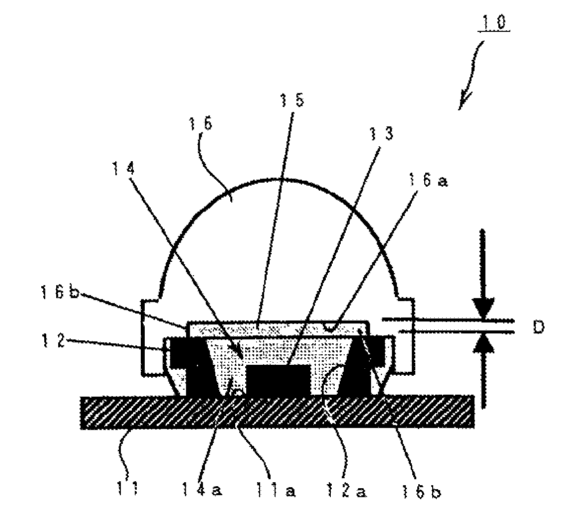
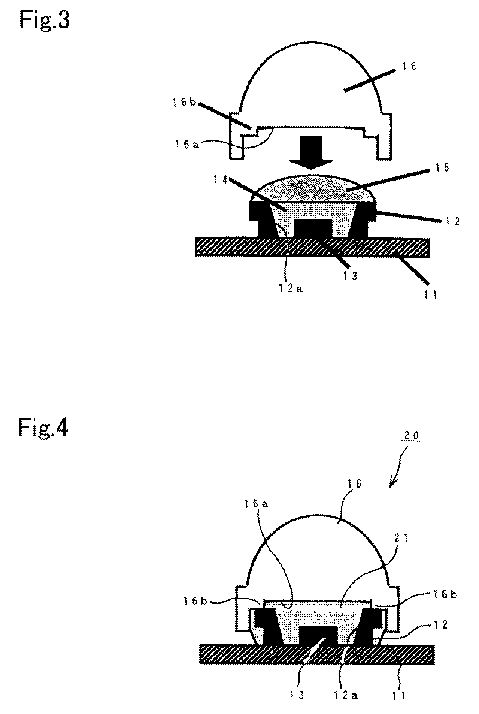
[0038]The first exemplary embodiment of the disclosed subject matter will now be described in detail with reference to FIG. 1 and FIG. 2. FIG. 1 is a cross-sectional view of a first exemplary embodiment made in accordance with principles of the disclosed subject matter and FIG. 2 is a bottom view showing an optical lens of the semiconductor light-emitting device shown in FIG. 1.

[0039]The semiconductor light-emitting device 10 can include: a base board 11 having a pair of chip mounting portions 11a; a reflector 12 that is formed in a substantially tubular shape with a cavity 12a, and disposed on the base board so as to enclose the pair of chip mounting portions 11a in the cavity 12a; a semiconductor light-emitting chip 13 that is mounted on the pair of chip mounting portions 11a, which are exposed on a bottom surface of the cavity 12a; an encapsulating resin 14 disposed in the cavity 12a of the reflector 12; a spacer 15 disposed over the reflector 12 that includes the encapsulating r...


PUM


Abstract

A reliable semiconductor light-emitting device and a method for manufacturing the same can be provided in which peeling can be prevented in a phase boundary, and optical axis positional errors between the optical lens and a semiconductor light-emitting chip can be reduced or prevented. The semiconductor light-emitting device can include a base board having at least one chip, a reflector fixed on the base board so as to enclose the chip, and an encapsulating resin disposed in the reflector. An optical lens can include a concave-shaped cavity that has an inner corner surface having a plurality of convex portions thereon. The optical lens can be located adjacent the reflector by contacting the lens with a top surface of the reflector so as to enclose the reflector. A spacer that is disposed between the concave-shaped cavity and the reflector can ease a stress that is generated due to temperature changes.

Description

[0001]This application claims the priority benefit under 35 U.S.C. §119 of Japanese Patent Application No. 2006-137258 filed on May 17, 2006, which is hereby incorporated in its entirety by reference.BACKGROUND[0002]1. Field[0003]The presently disclosed subject matter relates to semiconductor light-emitting devices including LEDs, laser diodes, etc. and to a manufacturing method for the same. More particularly, the disclosed subject matter relates to semiconductor light-emitting devices as described above that emit light through an optical lens and to the manufacturing method for these devices.[0004]2. Description of the Related Art[0005]A conventional semiconductor light-emitting device that emits light through an optical lens, for example, is disclosed in Patent Document No. 1 (Japanese Patent No. 3,492,178). According to Patent Document No. 1, and as shown in FIG. 8, a pair of lead frames 2a, 2b is insert-formed in a casing 1 that includes a cavity 1a for reflecting the light of ...

Claims


Application Information

Patent Timeline
Patent Type & Authority Patents(United States)
IPC IPC(8): H01L33/54H01L33/60H01L33/12H01L33/50H01L33/56H01L33/62
CPCH01L33/58H01L2924/0002H01L2924/00
Inventor HARADA, MITSUNORISATO, MASANORI
Owner STANLEY ELECTRIC CO LTD
Why Eureka
Try Eureka