Semiconductor device having increased gate length implemented by surround gate transistor arrangements

a technology of semiconductor devices and transistors, applied in semiconductor devices, solid-state devices, electrical devices, etc., can solve the problem of difficult to form an sgt having a gate length greater than the gate length ls of the unit sg

Active Publication Date: 2012-07-03
UNISANTIS ELECTRONICS SINGAPORE PTE LTD
View PDF32 Cites 40 Cited by
  • Summary
  • Abstract
  • Description
  • Claims
  • Application Information

AI Technical Summary

Benefits of technology

[0018]Preferably, in the semiconductor device according the second aspect of the present invention, the composite MOS transistor is formed by arranging in parallel a plurality of sets of the series-connected first to third MOS transistors having a gate electrode length three times greater than that of each of the first to third MOS transistors, and wherein the composite MOS transistor is configured to have a commonized gate electrode, a commonized source electrode and a commonized drain electrode to enhance a drive current.
[0022]Preferably, in the semiconductor device according the third aspect of the present invention, the composite MOS transistor is formed by arranging in parallel a plurality of sets of the series-connected first to fourth MOS transistors having a gate electrode length four times greater than that of each of the first to fourth MOS transistors, and wherein the composite MOS transistor is configured to have a commonized gate electrode, a commonized source electrode and a commonized drain electrode to enhance a drive current.
[0028]Preferably, in the semiconductor device according the fourth aspect of the present invention, the inverter is formed by arranging in parallel a plurality of sets of the two composite MOS transistors comprising the first to forth MOS transistors and each having a gate electrode length two times greater than that of each of the first to fourth MOS transistors, and wherein the inverter is configured to have a commonized gate electrode, a commonized source electrode and a commonized drain electrode to enhance a drive current.
[0036]Preferably, in the semiconductor device according the fifth aspect of the present invention, the inverter is formed by arranging in parallel a plurality of sets of the two composite MOS transistors comprising the first to sixth MOS transistors and each having a gate electrode length three times greater than that of each of the first to sixth MOS transistors, and wherein the inverter is configured to have a commonized gate electrode, a commonized source electrode and a commonized drain electrode to enhance a drive current.
[0047]As above, although it is difficult to form an SGT having a gate length greater than a gate length of a unit SGT due to a basic structure of the unit SGT, the present invention makes it possible to design a composite SGT having a gate length greater than the minimum gate length of the unit SGT, and a circuit using the composite SGT.

Problems solved by technology

However, due to a basic structure of an elemental or unit SGT, it is difficult to form an SGT having a gate length greater than a gate length Ls of the unit SGT.

Method used


Image

  • Semiconductor device having increased gate length implemented by surround gate transistor arrangements
  • Semiconductor device having increased gate length implemented by surround gate transistor arrangements
  • Semiconductor device having increased gate length implemented by surround gate transistor arrangements

Examples


first embodiment

[0098]A structure of a composite SGT having a gate length two times greater than a gate length Ls of a unit SGT (i.e., having a gate length of 2 Ls) will be shown below.

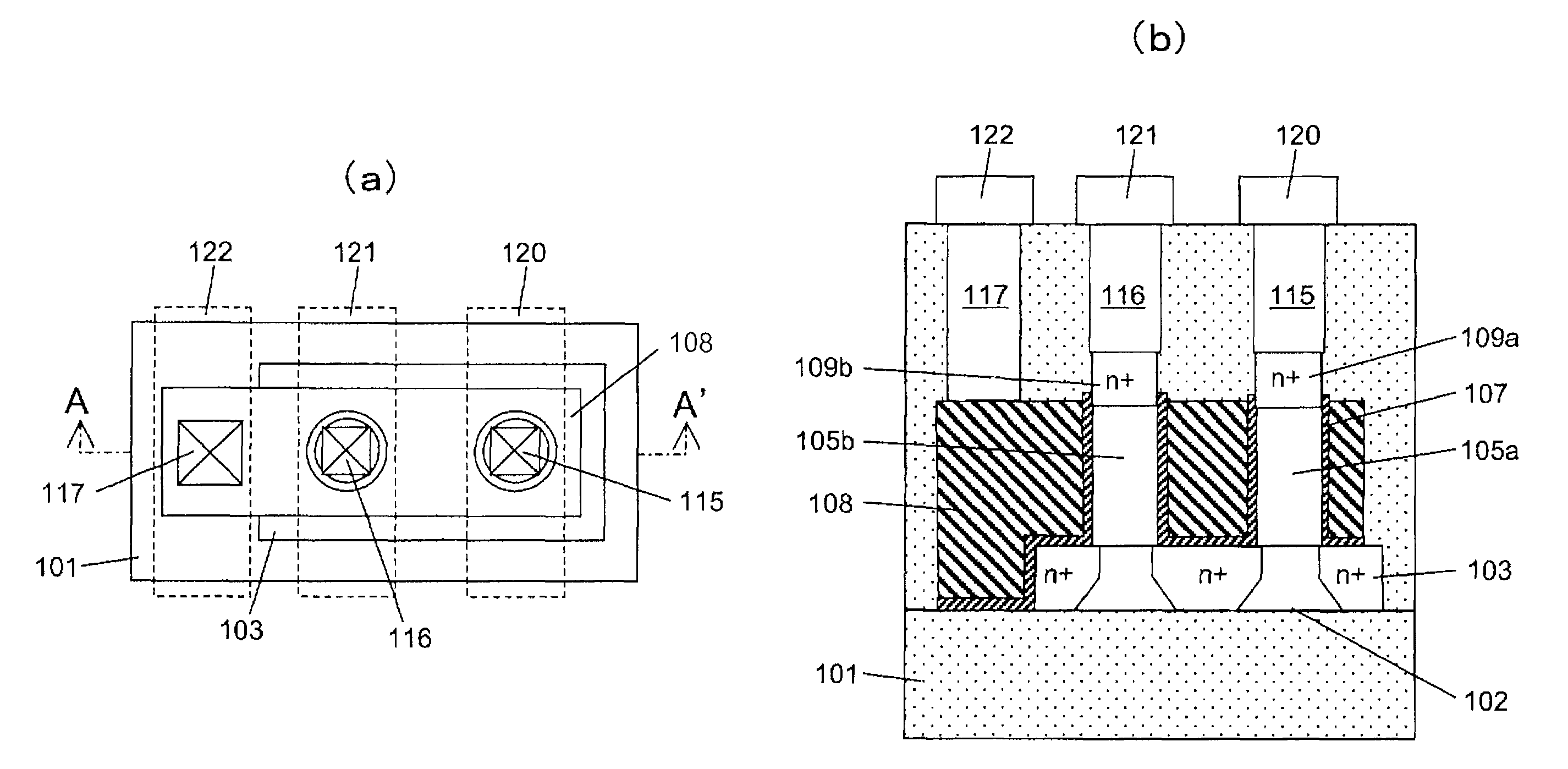
[0099]FIG. 1(a) is a top plan view showing a composite NMOS SGT having a gate length of 2 Ls, according to a first embodiment of the present invention, and FIG. 1(b) is a sectional view taken along the cutting-plane line A-A′ in FIG. 1(a). With reference to FIGS. 1(a) and 1(b), the composite NMOS SGT having a gate length of 2 Ls will be described below.

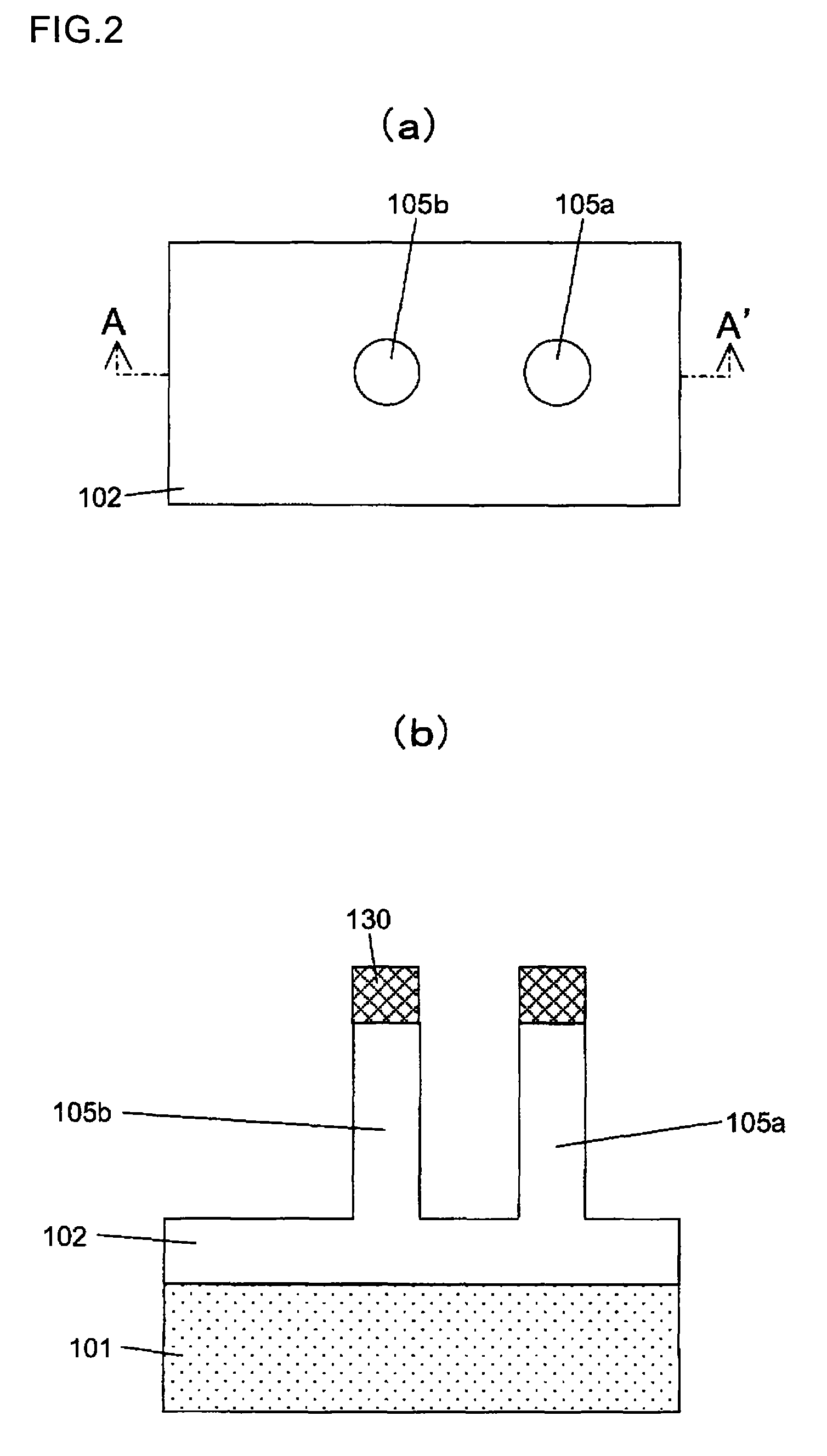
[0100]A planar silicon layer 102 is formed on a buried oxide film layer 101, and two pillar-shaped silicon layers 105a, 105b are formed on the planar silicon layer 102. An N+ lower diffusion layer 103 is formed in the planar silicon layer 102 underneath the pillar-shaped silicon layers 105a, 105b. A gate dielectric film 107 and a gate electrode 108 are formed around the pillar-shaped silicon layers 105a, 105b. The gate electrode 108 is connected to an interconnection l...

second embodiment

[0111]FIG. 10 is a top plan view showing a composite NMOS SGT which is formed by connecting in parallel a plurality of sets of series-connected two unit SGTs, to having a gate length of 2 Ls, according to a second embodiment of the present invention. In the second embodiment, a plurality of composite SGTs each fabricated as shown in FIGS. 1(a) and 1(b) to have a gate length of 2 Ls are connected in parallel so as to form a transistor having a large drive current.

[0112]With reference to FIG. 10, the composite NMOS SGT according to the second embodiment will be specifically described below.

[0113]A silicon layer 202 are formed on a buried oxide layer 201 in parallel with each other with respect to a row direction. A plurality of (e.g., five) sets of series-connected two pillar-shaped silicon layers 205a, 205b are formed on respective ones of the planar silicon layers 202, and an N+ lower diffusion layer 203 is formed in each of the planar silicon layers 202 underneath the pillar-shaped...

third embodiment

[0118]A structure of a composite SGT having a gate length three times greater than a gate length Ls of a unit SGT (i.e., having a gate length of 3 Ls) will be shown below. FIG. 12(a) is a top plan view showing a composite NMOS SGT having a gate length of 3 Ls, according to a third embodiment of the present invention, and FIG. 12(b) is a sectional view taken along the cutting-plane line A-A′in FIG. 12(a). With reference to FIGS. 12(a) and 12(b), the composite NMOS SGT having a gate length of 3 Ls will be described below.

[0119]A first planar silicon layer 402a and a second planar silicon layer 402b are formed on a buried oxide film layer 401. A pillar-shaped silicon layer 405a is formed on the first planar silicon layer 402a, and two pillar-shaped silicon layers 405b, 405c are formed on the second planar silicon layer 402b. An N+ lower diffusion layer 403a is formed in the first planar silicon layer 402a, and an N+ lower diffusion layer 403b is formed in the second planar silicon laye...


PUM


Abstract

In a vertical transistor comprising a pillar-shaped semiconductor layer and a gate electrode formed around the pillar-shaped semiconductor layer, it is difficult to form a transistor having a gate length greater than that of the vertical transistor. The present invention provides a semiconductor device which comprises two vertical transistors comprising first and second pillar-shaped semiconductor layers each formed on a first diffusion layer on a substrate. The vertical transistors have a common gate electrode. A first upper diffusion layer formed on a top of the first pillar-shaped semiconductor layer is connected to a source electrode, and a second upper diffusion layer formed on a top of the second pillar-shaped semiconductor layer is connected to a drain electrode. The vertical transistors are connected in series to operate as a composite transistor having a gate length two times greater than that of each of the vertical transistors.

Description

RELATED APPLICATIONS[0001]Pursuant to 35 U.S.C. §119(e), this application claims the benefit of the filing date of Provisional U.S. Patent Application Ser. No. 61 / 214,583 filed on Apr. 24, 2009. This application also claims priority under 35 U.S.C. §119(a) to JP2009-100745 filed on Apr. 17, 2009. The entire contents of these applications are hereby incorporated by reference.BACKGROUND OF THE INVENTION[0002]1. Field of the Invention[0003]The present invention relates to a semiconductor device, and more particularly to an SGT (Surrounding Gate Transistor) which is a vertical MOS transistor comprising a pillar-shaped semiconductor layer having a sidewall serving as a channel region, and a gate electrode formed to surround the channel region.[0004]2 . Description of the Related Art[0005]With a view to achieving higher integration and higher performance of a semiconductor device, an SGT (Surrounding Gate Transistor) has been proposed which is a vertical transistor comprising a pillar-sha...

Claims


Application Information

Patent Timeline
Patent Type & Authority Patents(United States)
IPC IPC(8): H01L27/088
CPCH01L21/823828H01L21/823878H01L21/823885H01L21/84H01L27/092H01L27/1203H01L29/78642H01L2924/13091
Inventor MASUOKA, FUJIOARAI
Owner UNISANTIS ELECTRONICS SINGAPORE PTE LTD
Why Eureka
Try Eureka