Method for removing threshold voltage adjusting layer with external acid diffusion process

a threshold voltage and acid diffusion technology, applied in the field of semiconductor device fabrication, can solve the problems of increasing the dose of impurities increasing the current of the substrate upon application of substrate voltage,

Inactive Publication Date: 2012-07-24
ELPIS TECH INC
View PDF8 Cites 100 Cited by
  • Summary
  • Abstract
  • Description
  • Claims
  • Application Information

AI Technical Summary

Problems solved by technology

Threshold voltage control using only this technique, e.g., only through adjustment of the amount of the channel impurity, however, raises nonconformities such that an increase in the dose of the impurity to be doped into the channel region may lower ON-state current due to scattering by the impurity, may increase the Gate-Induced Drain Leakage (GIDL) current, and may increase substrate current upon application of substrate voltage.
Although high k dielectrics provide improvements over conventionally used silicon oxide as the gate insulating film in a FET device, the use of the same is not without problems.
For example, FET devices including high k gate dielectrics exhibit a non-ideal threshold voltage when the device is used.
Although this problem, e.g., threshold voltage shift from an ideal value, is exhibited for both pMOSFET and nMOSFET devices, it is more pronounced with nMOSFET devices.
Although such threshold voltage adjusting techniques have been proposed, threshold voltage centering still remains a challenge in such devices due to the difficulty of integrating band-edge metals for nFETs and pFETs.
The undercutting of the threshold voltage adjusting layer is undesirable since the dimension of the final gate stack would deviate from required criteria.

Method used


Image

  • Method for removing threshold voltage adjusting layer with external acid diffusion process
  • Method for removing threshold voltage adjusting layer with external acid diffusion process
  • Method for removing threshold voltage adjusting layer with external acid diffusion process

Examples


Embodiment Construction

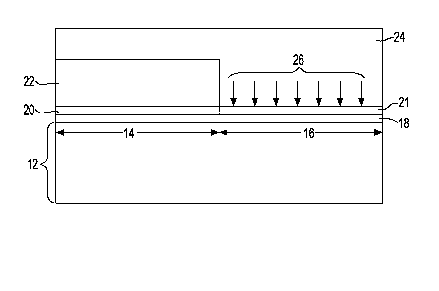
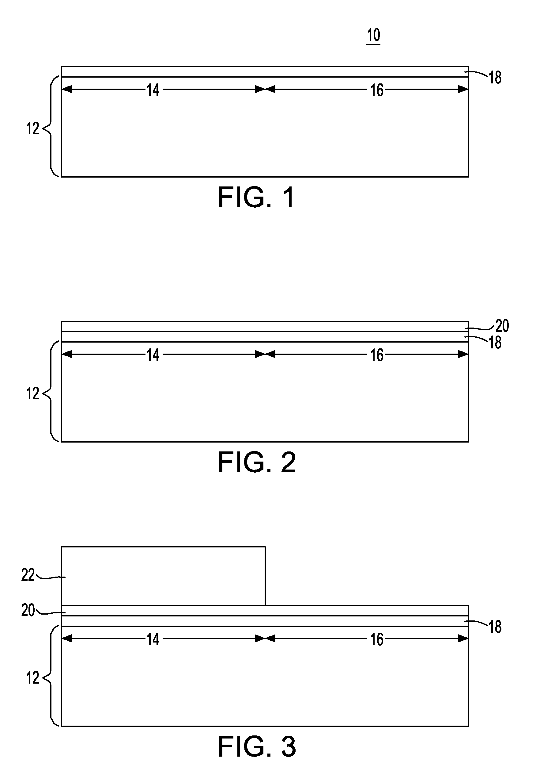
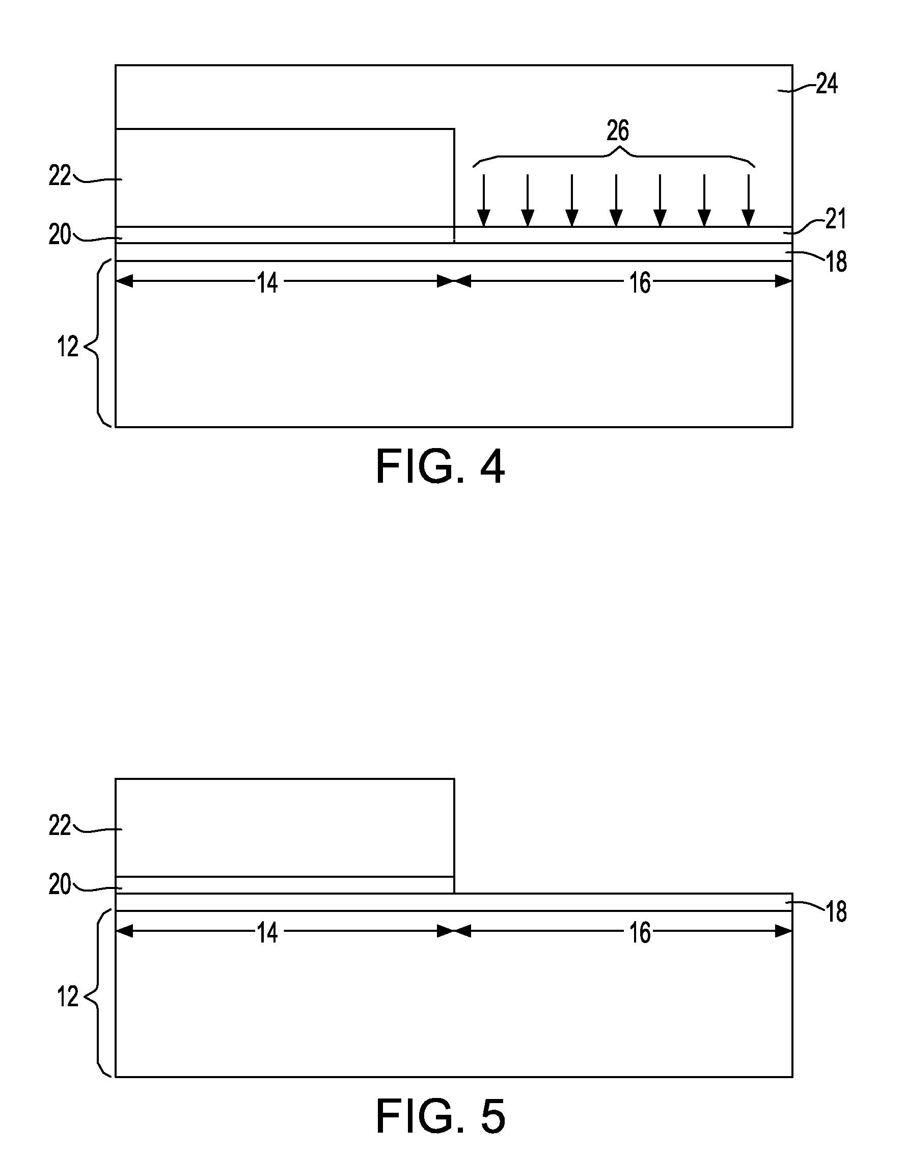
[0020]The present invention, which provides a method for patterning a threshold voltage adjusted gate stack utilizing an external acid diffusion process to remove unwanted threshold voltage adjusting material from preselected device regions, will now be described in greater detail by referring to the following discussion and drawings that accompany the present application. It is noted that the drawings of the present application are provided for illustrative purposes only and, as such, the drawings are not drawn to scale.

[0021]In the following description, numerous specific details are set forth, such as particular structures, components, materials, dimensions, processing steps and techniques, in order to provide a thorough understanding of the present invention. However, it will be appreciated by one of ordinary skill in the art that the invention may be practiced without these specific details. In other instances, well-known structures or processing steps have not been described i...


PUM

PropertyMeasurementUnit
thicknessaaaaaaaaaa
thicknessaaaaaaaaaa
dielectric constantaaaaaaaaaa

Abstract

The present invention provides a method of forming a threshold voltage adjusted gate stack in which an external acid diffusion process is employed for selectively removing a portion of a threshold voltage adjusting layer from one device region of a semiconductor substrate. The external acid diffusion process utilizes an acid polymer which when baked exhibits an increase in acid concentration which can diffuse into an underlying exposed portion of a threshold voltage adjusting layer. The diffused acid reacts with the exposed portion of the threshold voltage adjusting layer providing an acid reacted layer that can be selectively removed as compared to a laterally adjacent portion of the threshold voltage adjusting layer that is not exposed to the diffused acid.

Description

FIELD OF THE INVENTION[0001]The present invention relates to semiconductor device fabrication, and more particularly to a method of forming a semiconductor device including a threshold voltage adjusted gate stack in which an external acid diffusion process is employed in patterning the threshold voltage adjusted gate stack.BACKGROUND OF THE INVENTION[0002]In semiconductor devices including field effect transistors (FETs), threshold voltage of the transistors has been conventionally controlled by doping an impurity into the channel region and by appropriately adjusting the dose amount. Threshold voltage control using only this technique, e.g., only through adjustment of the amount of the channel impurity, however, raises nonconformities such that an increase in the dose of the impurity to be doped into the channel region may lower ON-state current due to scattering by the impurity, may increase the Gate-Induced Drain Leakage (GIDL) current, and may increase substrate current upon app...

Claims


Application Information

Patent Timeline
Patent Type & Authority Patents(United States)
IPC IPC(8): H01L21/8238H01L21/31
CPCH01L21/31122H01L21/823842H01L21/823857
Inventor CHEN, KUANG-JUNGDONATON, RICARDO A.HUANG, WU-SONGLI, WAI-KIN
Owner ELPIS TECH INC
Why Eureka
Try Eureka