Method and apparatus for detecting foreign materials and storage medium

a technology for foreign materials and storage media, applied in material analysis, semiconductor/solid-state device testing/measurement, instruments, etc., can solve the problems of difficult detection of particles, deterioration of product substrate yield, and inability to detect quality, etc., to achieve stable and accurate detection and suitable inspection

Inactive Publication Date: 2012-08-14
TOKYO ELECTRON LTD
View PDF10 Cites 0 Cited by
  • Summary
  • Abstract
  • Description
  • Claims
  • Application Information

AI Technical Summary

Benefits of technology

[0008]In view of the above, the present invention provides a method and an apparatus for detecting foreign materials attached onto a substrate surface, which can stably and accurately detect even fine foreign materials smaller than a detection limit of a conventional measuring device and can be widely used and suitable for inspection of mass-produced substrates, and a storage medium.

Problems solved by technology

The particles are foreign materials to an integrated circuit, making the quality thereof unacceptable.
Therefore, it is expected that it will be difficult to detect particles as foreign materials attached onto a wafer surface in the near future.
In that case, it is not possible to manage the condition in an accommodation chamber of a substrate processing apparatus for performing a predetermined process on a substrate such as a wafer or the like, so that a yield of product substrates deteriorates.
In the prior art, however, the ice crystal is not always stable.
However, a reaction product of cyanoacrylate and water (snow crystal) is stable and thus cannot be decomposed.
Accordingly, the substrate that has been subjected to the surface inspection cannot be restored to the original state, which prevents the inspected substrate from being subjected to another inspection or from being used as a product.

Method used


Image

  • Method and apparatus for detecting foreign materials and storage medium
  • Method and apparatus for detecting foreign materials and storage medium
  • Method and apparatus for detecting foreign materials and storage medium

Examples


Embodiment Construction

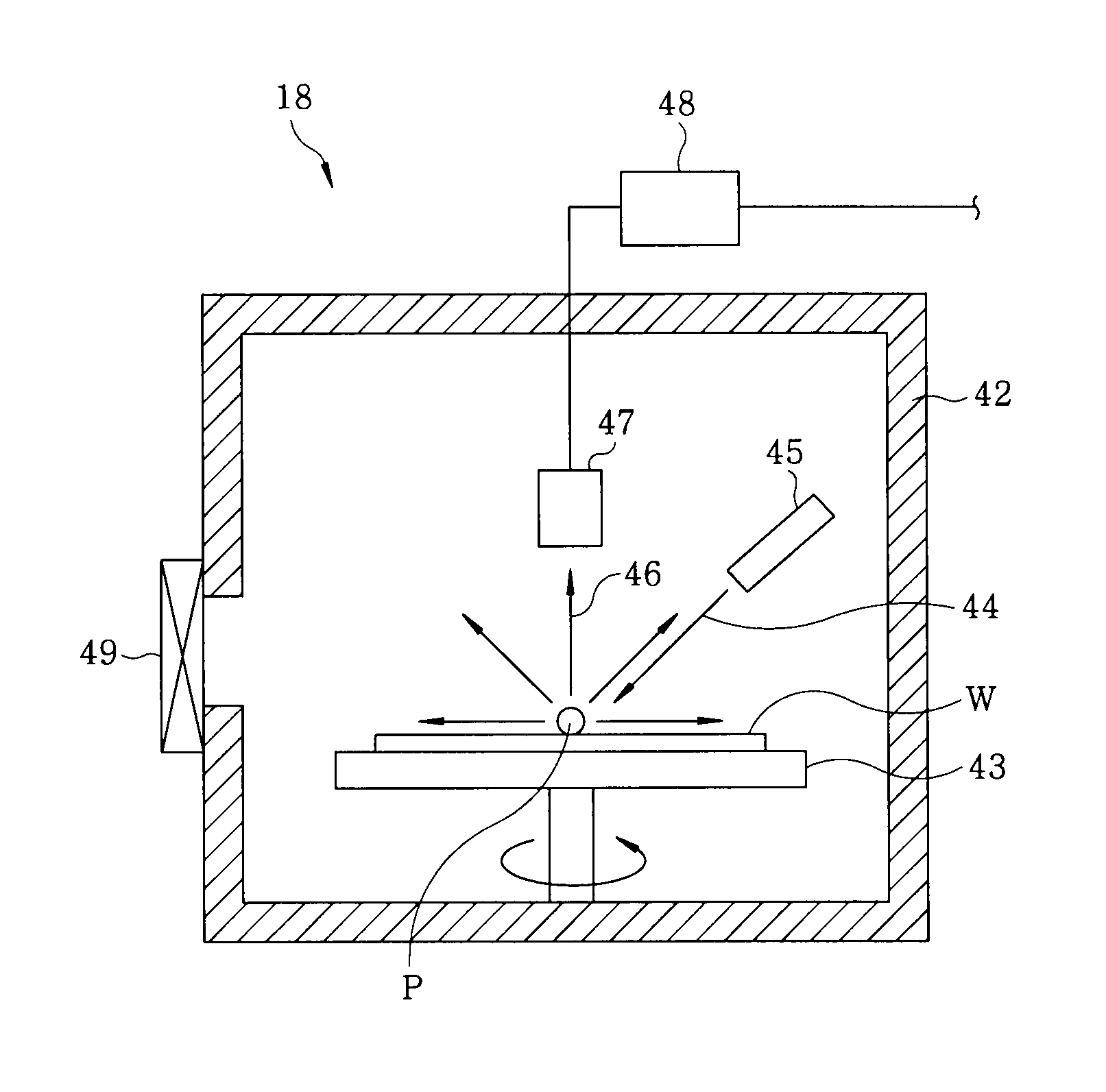
[0017]The present inventors have performed various examinations on a method for detecting particles as foreign materials attached to a substrate surface and have found that if the particles are enlarged or emphasized, they can be detected by a conventional measuring device, e.g., an optical microscope, an electron microscope, a laser light scattering method or the like. Based on the above, the present inventors have researched a method for enlarging or emphasizing particles attached to a substrate surface and a method for detecting the particles. As a result, the present inventors have found that the particles are emphasized by spraying an organic solvent or an oil-phase material containing a halogen element onto the substrate surface and condensing the sprayed organic solvent or oil-phase material around the particles by controlling a temperature of the substrate surface to a predetermined temperature.

[0018]In other words, the foreign material detecting method of the present invent...


PUM

PropertyMeasurementUnit
particle sizeaaaaaaaaaa
widthaaaaaaaaaa
particle sizeaaaaaaaaaa

Abstract

A foreign material detecting method for detecting a foreign material attached to a substrate surface includes a spraying step of spraying an organic solvent or an oil-phase material containing a halogen element to the substrate surface, a condensing step of emphasizing the foreign material by condensing the sprayed organic solvent or oil-phase material around the foreign material attached to the substrate surface by controlling a temperature of the substrate surface, and a surface inspecting step of detecting the foreign material emphasized by the condensation of the organic solvent or the oil-phase material by a surface inspecting device.

Description

FIELD OF THE INVENTION[0001]The present invention relates to a method and an apparatus for detecting foreign materials and a storage medium; and, more particularly, to a method for detecting foreign materials such as polymers or the like attached to a substrate surface by emphasizing the foreign materials through a pre-process and inspecting the substrate surface.BACKGROUND OF THE INVENTION[0002]The attachment of particles onto a surface of a semiconductor substrate (hereinafter, referred to as “wafer”) is one of the reasons for deteriorating a production yield in a semiconductor manufacturing process. The particles are foreign materials to an integrated circuit, making the quality thereof unacceptable. Conventionally, a particle size that deteriorates the production yield is, e.g., about 50 nm to 70 nm, and can be detected by a surface inspection device such as a Surfscan or the like.[0003]Recently, a trend towards high integration of chips is accelerated in a semiconductor industr...

Claims


Application Information

Patent Timeline
Patent Type & Authority Patents(United States)
IPC IPC(8): G01N21/00
CPCG01N21/91G01N21/94G01N21/9501H01L21/67288H01L22/00
Inventor MORIYA, TSUYOSHINAGAIKE, HIROSHIYAKUSHIJI, HIDEAKI
Owner TOKYO ELECTRON LTD
Why Eureka
Try Eureka