Method of manufacturing semiconductor device, and semiconductor device

a manufacturing method and technology of semiconductor devices, applied in the direction of semiconductor devices, electrical appliances, transistors, etc., to achieve the effect of reducing the implantation mask

Active Publication Date: 2012-09-18
RENESAS ELECTRONICS CORP
View PDF12 Cites 14 Cited by
  • Summary
  • Abstract
  • Description
  • Claims
  • Application Information

AI Technical Summary

Benefits of technology

[0018]In accordance with the method of manufacturing the semiconductor device according to the present invention, it is possible to reduce implantation masks for forming the halo regions of the transistor of the first conductivity type and the transistor of the second conductivity type.

Problems solved by technology

However, in the SRAM including the access transistors described above has the following problem.

Method used


Image

  • Method of manufacturing semiconductor device, and semiconductor device
  • Method of manufacturing semiconductor device, and semiconductor device
  • Method of manufacturing semiconductor device, and semiconductor device

Examples


first example

[0236]In a first example, the case will be described where, using the individual resist masks described in Embodiment 1, boron and carbon are implanted.

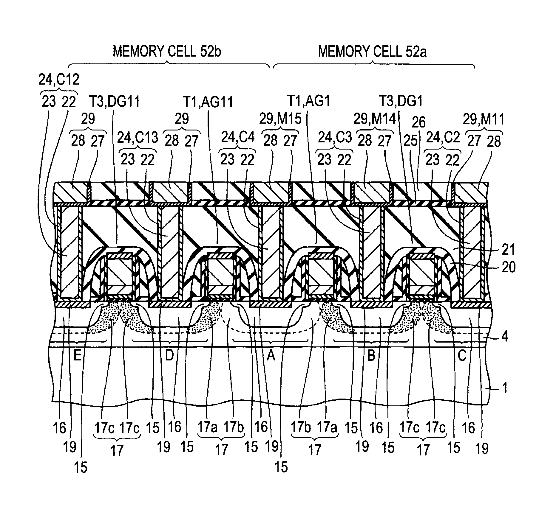
[0237]First, a description will be given of an equivalent circuit of a SRAM memory cell. As shown in FIG. 55, in the access transistors T1 and T2 in the semiconductor device according to the first example, the respective pairs of halo regions 17 formed therein include halo regions 17g coupled to the storage nodes SN1 and SN2 and halo regions 17h coupled to the bit lines BL and / BL, and the impurity concentrations of the halo regions 17g are set higher than the impurity concentrations of the halo regions 17h. In the drive transistors T3 and T4, the impurity concentrations of the respective pairs of halo regions 17 (17j) formed therein are set the same as the impurity concentrations of the halo regions 17g. Into the halo regions 17g and 17j among the halo regions 17g, 17h, and 17j, as an impurity, carbon is implanted in addition to bor...

second example

[0253]In a second example, the case will be described where, using the individual resist masks described in Embodiment 2, boron (p-type impurity) and carbon are implanted. As shown in FIG. 66, in the access transistors T1 and T2 of the semiconductor device according to the second example, the respective pairs of halo regions 17 formed therein include halo regions 17k coupled to the storage nodes SN1 and SN2 and halo regions 17m coupled to the bit lines BL and / BL, and the impurity concentrations of the halo regions 17k are set higher than the impurity concentrations of the halo regions 17m. In the drive transistors T3 and T4, the respective pairs of halo regions 17 (17p and 17n) formed therein include halo regions 17n coupled to the storage nodes SN1 and SN2 and halo regions 17p coupled to the ground potential, and the impurity concentrations of the halo regions 17n are set higher than the impurity concentrations of the halo regions 17p. Into the halo regions 17k and 17n among the h...


PUM


Abstract

There are provided a method of manufacturing a semiconductor device which achieves a reduction in implantation masks, and such a semiconductor device. By implanting boron into NMOS regions using a resist mask and another resist mask as the implantation masks, p-type impurity regions serving as the halo regions of access transistors and drive transistors are formed. By further implanting phosphorus or arsenic into a PMOS region using another resist mask as the implantation mask, n-type impurity regions serving as the halo regions of load transistors are formed.

Description

CROSS-REFERENCE TO RELATED APPLICATIONS[0001]The disclosure of Japanese Patent Application No. 2010-24513 filed on Feb. 5, 2010 including the specification, drawings and abstract is incorporated herein by reference in its entirety.BACKGROUND OF THE INVENTION[0002]The present invention relates to a method of manufacturing a semiconductor device and the semiconductor device, and particularly to a method of manufacturing a semiconductor device including a SRAM and such a semiconductor device.[0003]As a form of a semiconductor device, there is a semiconductor device called a SOC (System On Chip). In a semiconductor device of this type, a plurality of logic circuits, memory cells, and the like are mounted on one chip. A description will be given herein of a semiconductor device in which a SRAM (Static Random Access Memory) is applied to a memory cell of such a semiconductor device.[0004]A SRAM memory cell includes a flip-flop in which two inverters are cross-coupled, and two access trans...

Claims


Application Information

Patent Timeline
Patent Type & Authority Patents(United States)
IPC IPC(8): H01L27/088H01L21/8234
CPCH01L21/823412H01L27/1104H01L27/11H10B10/00H10B10/12
Inventor NIL, KOJIIGARASHI, MOTOSHIGE
Owner RENESAS ELECTRONICS CORP
Why Eureka
Try Eureka