
Semiconductor device socket

a technology of semiconductor devices and sockets, applied in the direction of coupling contact members, coupling device connections, instruments, etc., can solve the problems of inadvisable preparation of spare test boards, increased equipment costs, and relatively long period of time, and achieve the effect of short period of time and easy operation

Active Publication Date: 2012-09-25
YAMAICHI ELECTRONICS
View PDF87 Cites 13 Cited by
  • Summary
  • Abstract
  • Description
  • Claims
  • Application Information

AI Technical Summary

Benefits of technology

[0014]In view of the above-described problems, the present invention aims to provide a semiconductor device socket for electrically connecting a semiconductor device that undergoes a test to a printed wiring board. The semiconductor device socket can replace only a defective IC socket with an easy work and in a short period of time, and prevent a fixed terminal portion of a contact terminal from applying an excessive contact pressure on a contact pad of a printed wiring board.
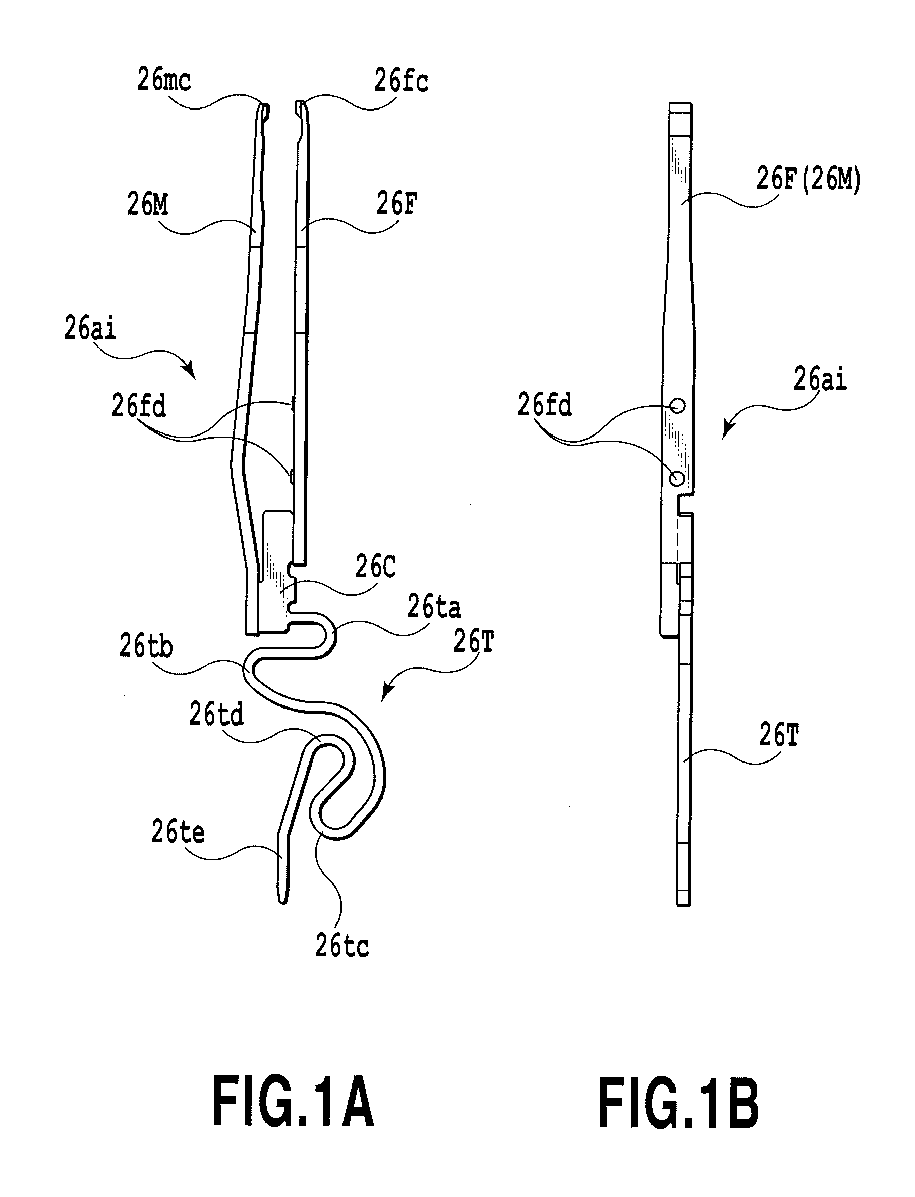
[0016]Therefore, according to the semiconductor device socket of the present invention, the contact terminal comprises a pair of movable contact pieces being elastic and pinching a terminal of the semiconductor device, a fixed side terminal having a curved portion and a contact point on one end of the curved portion, and a fixed portion for connecting proximal end portions of the pair of movable side contact pieces of the contact terminal to another end of the fixed side terminal, the curved portion formed to be continuous with each of the movable contact pieces and elastically displaceable in a direction orthogonal to the electrode surface of the wiring board, the contact point coming into contact with the electrode surface of the wiring board, the contact terminal for connecting the terminal of the semiconductor device electrically to the electrode surface of the wiring board. Accordingly, the semiconductor device socket of the present invention can replace only a defective IC socket with an easy operation and in a short period of time and prevent the fixed terminal portion of the contact terminal from applying an excessive contact pressure on a contact pad of the printed wiring board.

Problems solved by technology

To prepare the spare test board, however, is inadvisable because of an increase in equipment costs on the inspection line.
In addition, a soldering operation for the fixed terminals of the contact terminals consumes a relatively long period of time for a replacement operation, and moreover, the test board may be broken, leading to a drop in yield.
However, in the case of the above-described curved fixed terminal, it is difficult to adjust a spring constant because of the above-mentioned height restriction.
Hence there is a risk that an excessive contact pressure is applied to the contact pad on the printed wiring board.

Method used


Image

  • Semiconductor device socket
  • Semiconductor device socket
  • Semiconductor device socket

Examples


Embodiment Construction

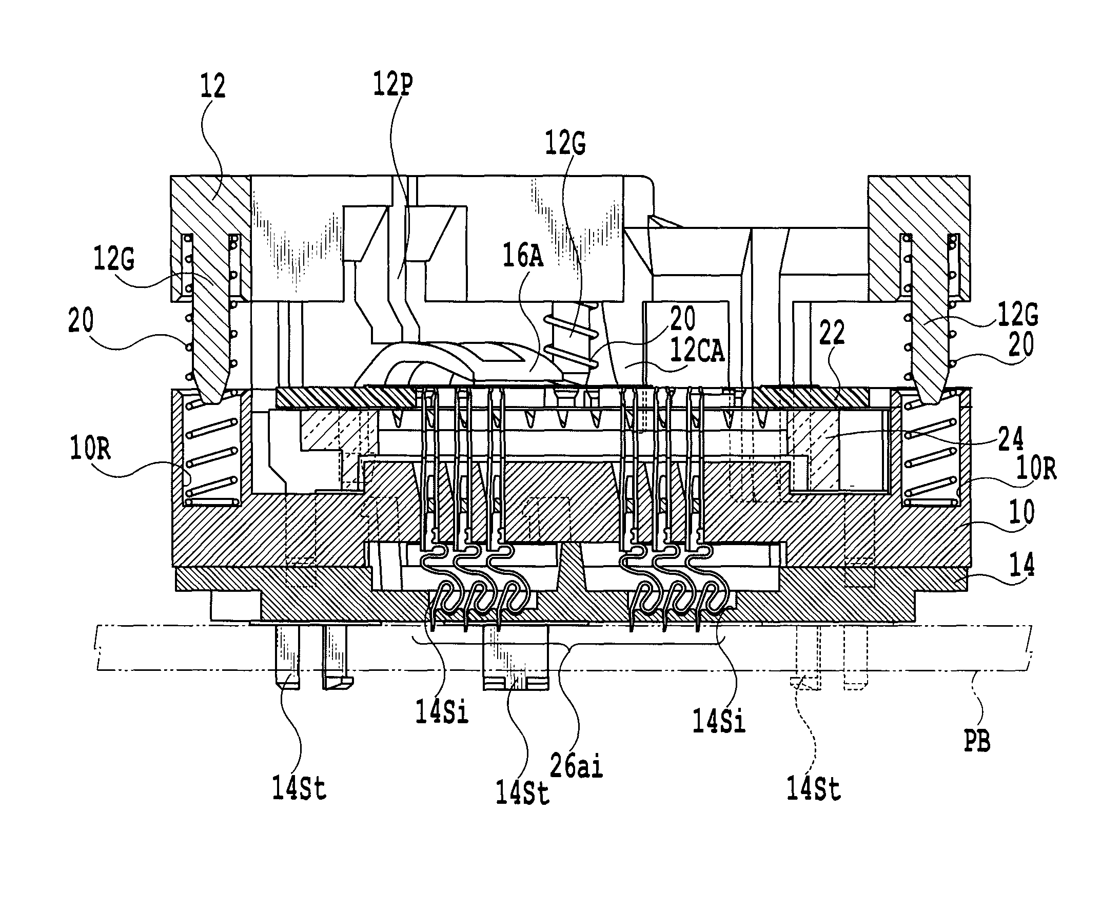
[0042]FIG. 3 shows an enlarged view of an example of a semiconductor device socket according to the present invention together with a printed wiring board serving as a test board. Besides, FIG. 3 represents one of a plurality of semiconductor device sockets to be disposed on the printed wiring board.

[0043]The semiconductor device sockets are of an open top type, for example, and are respectively disposed in predetermined positions on a conductive pattern formed on a printed wiring board PB having a predetermined board thickness. An electrode group PBE with which contact points of fixed side terminals of contact terminals to be described later are brought into contact is formed in a predetermined position on the conductive pattern as enlarge in FIG. 18A and FIG. 18B. In addition, substantially circular shaped holes (not shown) into which each fixed nib portions of the semiconductor device sockets to be described later are inserted are formed around the conductive pattern. Besides, th...


PUM


Abstract

A contact terminal (26ai) comprises: a pair of movable side contact pieces (26M) and (26F) which pinch or release a ball-like electrode portion (DVa) of a semiconductor device (DV); a fixed side terminal (26T) having on one end a contact point (26te) coming into contact with an electrode group (PBE) of a printed wiring board (PB); and a fixing portion (26C) which connects proximal end portions of the pair of elastic movable side contact pieces (26M) and (26F) to the other end of the fixed side terminal (26T). The fixed side terminal (26T) formed into a curved shape is elastic and has the one end thereof joined to the fixing portion (26C). The fixed side terminal (26T) is formed of a plurality of curved portions (26ta, 26tb, 26tc, and 26td) and the contact point (26te) provided continuous with one another.

Description

TECHNICAL FIELD[0001]The present invention relates to a semiconductor device socket for electrically connecting a semiconductor device that undergoes a test to a printed wiring board.BACKGROUND ART[0002]Generally, a semiconductor device to be mounted on an electronic device or the like undergoes, for example, a burn-in test, which is deemed to be effective for eliminating an integrated circuit having an infant mortality failures, by use of a semiconductor device socket in order to eliminate a potential defect of the semiconductor device at a stage before the semiconductor device is mounted.[0003]A semiconductor device socket used for the test is generally referred to as an IC socket and is disposed on a printed wiring board (a test board) as shown in Patent Document 1, for example. The printed wiring board is provided with an input-output unit for receiving and supplying signals. The input-output unit is assumed to receive a supply of a predetermined test voltage and to send an anom...

Claims


Application Information

Patent Timeline
Patent Type & Authority Patents(United States)
IPC IPC(8): H01R12/00H01R13/15
CPCG01R1/0466H01R13/193H01R13/2428G01R1/0483
Inventor SAKAI, TOORUKOUMI, KUNIYOSHI
Owner YAMAICHI ELECTRONICS
Learn More