Data sensing module and sensing circuit for flash memory

a data sensing module and flash memory technology, applied in the field of data sensing modules, can solve the problems of data read speed likely delayed, excessive load of sensing circuits, etc., and achieve the effect of increasing the data reading speed

Active Publication Date: 2012-10-09
WINBOND ELECTRONICS CORP
View PDF4 Cites 2 Cited by
  • Summary
  • Abstract
  • Description
  • Claims
  • Application Information

AI Technical Summary

Benefits of technology

[0007]The present invention is directed to a sensing circuit, which can be used in a flash memory to increase a data reading speed.
[0008]The present invention is directed to a data sensing module of a flash memory, which can increase a performance of a read operation of the flash memory.
[0012]Since the source of the first transistor is charged as the voltage of the drain of the first transistor being lower than the threshold voltage. Therefore, the performance of the data read operation can be increased.

Problems solved by technology

In the flash memory, since a large amount of memory cells are coupled to the sensing circuit, a great amount of parasitic capacitances are generally generated in the sensing circuit, which may lead to an excessive load of the sensing circuit, and accordingly the data read speed is probably delayed.

Method used


Image

  • Data sensing module and sensing circuit for flash memory
  • Data sensing module and sensing circuit for flash memory
  • Data sensing module and sensing circuit for flash memory

Examples


Embodiment Construction

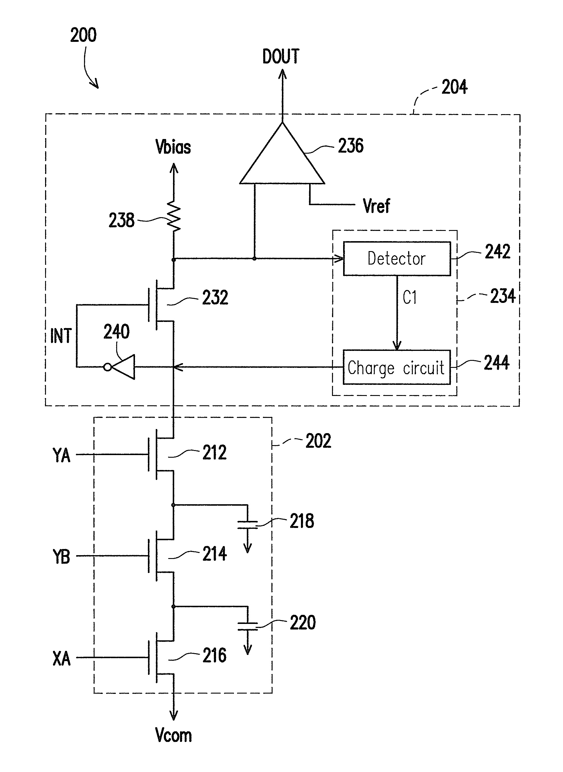
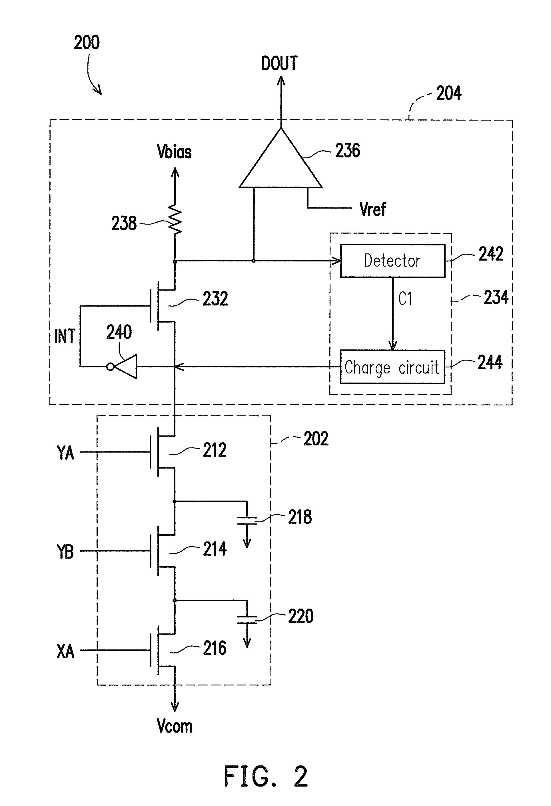
[0018]To fully convey the spirit of the present invention to those skilled in the art, a system structure of a flash memory is briefly described below.

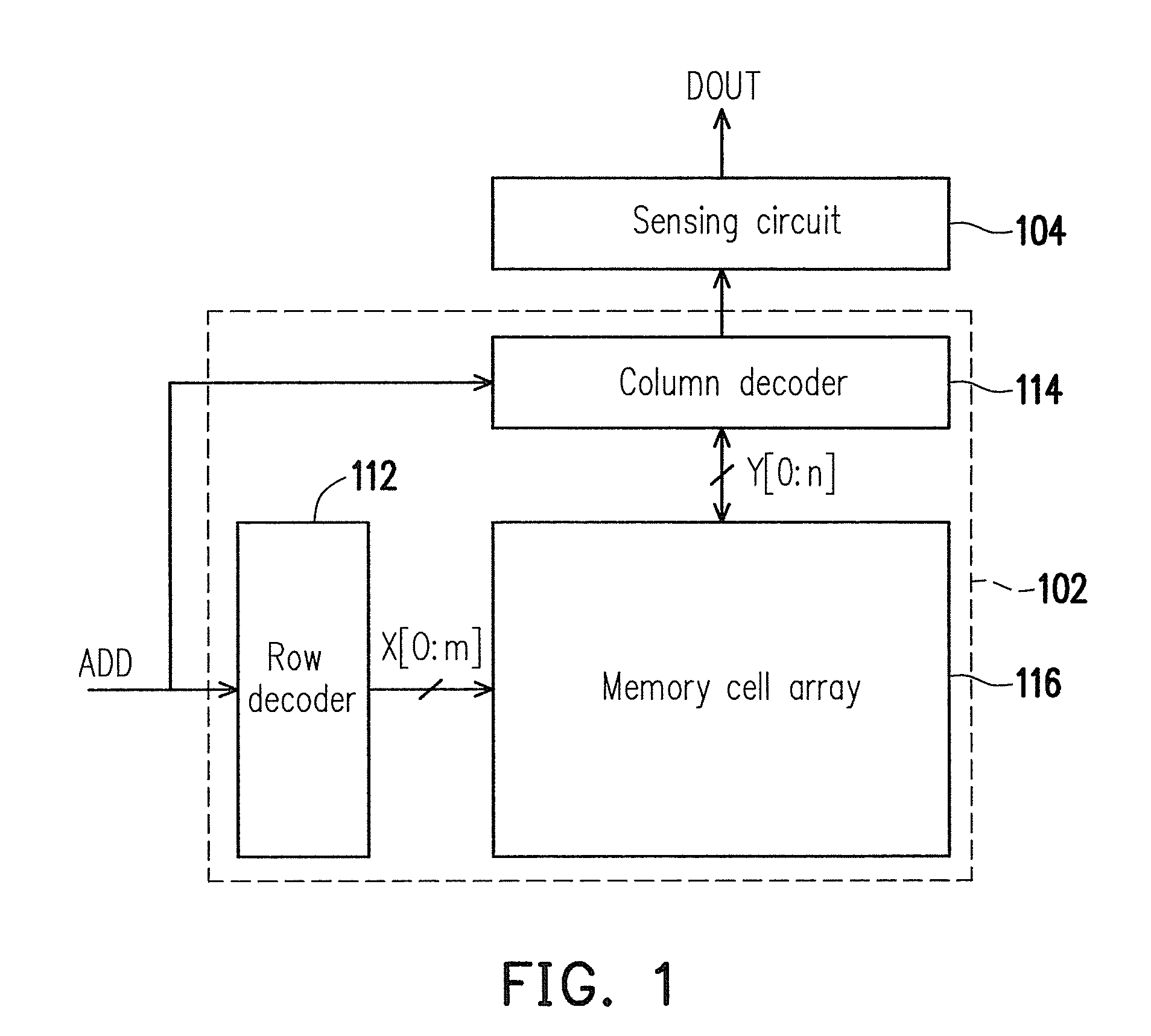
[0019]FIG. 1 is a block diagram of an internal sensing system of a flash memory. Referring to FIG. 1, a general flash memory includes a memory core circuit 102 and a sensing circuit 104. The memory core circuit 102 coupled to the sensing circuit 104 is used for receiving an address information ADD.

[0020]The memory core circuit 102 includes a row decoder 112, a column decoder 114 and a memory cell array 116. Wherein, the memory cell array 116 has a plurality of memory cells coupled to the row decoder 112 through a plurality of word lines X[0:m], and coupled to the column decoder 114 through a plurality of bit lines Y[0:n] respectively. The row decoder 112 and the column decoder 114 can respectively receive the address information ADD, and the column decoder 114 is further coupled to the sensing circuit 104.

[0021]When a data read operat...


PUM


Abstract

A sensing circuit for a flash memory is provided. The sensing circuit includes a first transistor, a detector, and a charge circuit. A drain of the first transistor is coupled to a bias, a gate thereof receives an inverted signal, and a source thereof receives a data. In addition, the drain of the first transistor is further coupled to the detector. Therefore, the detector detects a voltage of the drain of the first transistor. When the voltage of the drain is lower than a threshold voltage, the detector enables a control signal. The charge circuit charges the source of the first transistor when the control signal is enabled, until the voltage of the drain of the first transistor reaches the threshold voltage.

Description

BACKGROUND OF THE INVENTION[0001]1. Field of the Invention[0002]The present invention relates to a data sensing module. More particularly, the present invention relates to a data sensing module of a flash memory.[0003]2. Description of Related Art[0004]Data stored in a memory are mostly binary bits, and a device is assigned to record a state of each bit being 0 or 1, wherein such device is referred to as a memory cell. In the memory, a data write or read operation of the selected memory cell is determined by an output signal of a control circuit. During the write operation, a predetermined memory cell is selected, and then the data to be written is stored in the selected memory cell. Comparatively, during the read operation, a predetermined memory cell is also selected, and then the state of the stored bit represented by a current or a voltage is recognized by a sensing circuit.[0005]A flash memory is a random access memory capable of maintaining the stored data under a power-off st...

Claims


Application Information

Patent Timeline
Patent Type & Authority Patents(United States)
IPC IPC(8): G11C11/34G11C16/04
CPCG11C16/28
Inventor LIAO, WEI-CHIH
Owner WINBOND ELECTRONICS CORP
Why Eureka
Try Eureka