NAND flash memory data reading method and device and NAND flash memory

A data reading and flash memory technology, which is applied in the field of NAND flash memory, can solve the problems of long time consumption and slow data reading speed

Active Publication Date: 2016-06-15
GIGADEVICE SEMICON (BEIJING) INC
View PDF3 Cites 2 Cited by
  • Summary
  • Abstract
  • Description
  • Claims
  • Application Information

AI Technical Summary

Problems solved by technology

[0005] In view of this, an embodiment of the present invention provides a method and device for reading data from a NAND flash memory, and a NAND flash memory, so as to solve the problems of slow data reading speed and long time-consuming in the prior art

Method used


Image

  • NAND flash memory data reading method and device and NAND flash memory
  • NAND flash memory data reading method and device and NAND flash memory
  • NAND flash memory data reading method and device and NAND flash memory

Examples


Embodiment 1

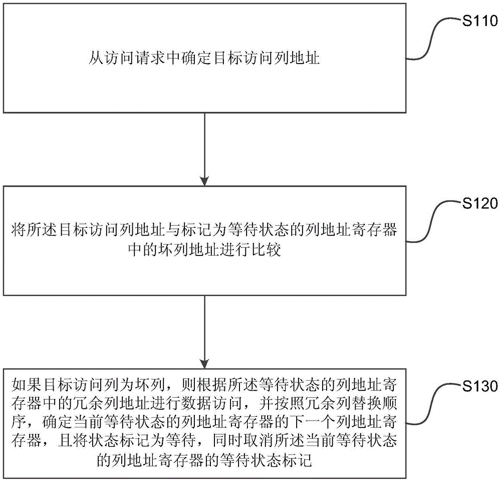
[0031] Embodiment 1 of the present invention provides a method for reading data from a NAND flash memory. The method can be executed by a device for reading data from a NAND flash memory. The device can be implemented by software and / or hardware, and can generally be integrated in a NAND flash memory. figure 2 It is a schematic flowchart of a data reading method of a NAND flash memory according to Embodiment 1 of the present invention. Such as figure 2 As shown, the method includes:

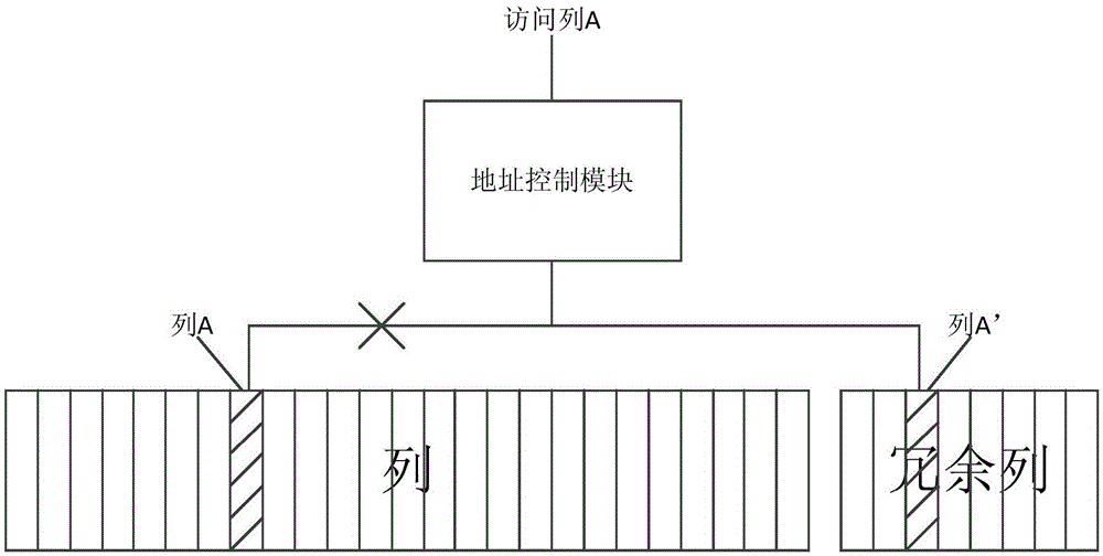
[0032] S110. Determine a target access column address from the access request.

[0033] Here, the user's access request may be an access request for pictures and text, or an access request for audio, video, etc., which is not limited here. Preferably, an access address register can be set in the NAND flash memory, and the access address register is used to store the user's target access column address. Among them, the register is a high-speed storage unit with limited storage capacity, usual...

Embodiment 2

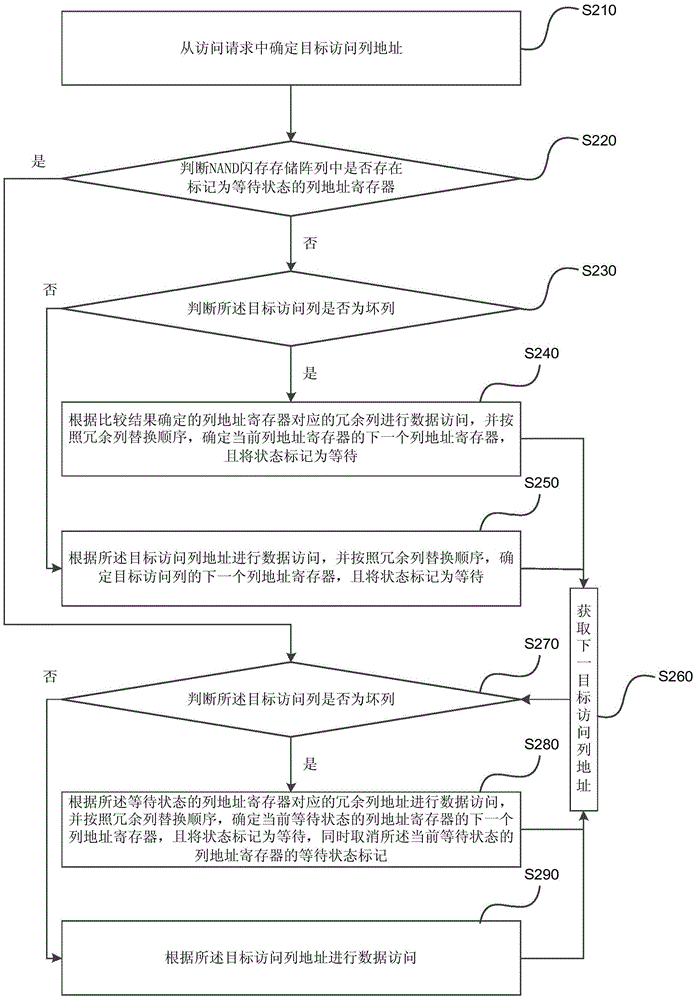
[0049] image 3 It is a schematic flow diagram of a data reading method of a NAND flash memory provided by Embodiment 2 of the present invention. This embodiment is optimized on the basis of the above embodiments. Further, the target access column address and the column marked as waiting state Before the bad column address in the address register is compared, also include: if there is no column address register marked as waiting state, then compare the target access column address with the bad column address in each column address register; if the target access If the column is a bad column, perform data access to the redundant column corresponding to the column address register determined by the comparison result, and determine the next column address register of the current column address register according to the replacement sequence of the redundant column, and mark the status as waiting; If the target access column is a normal column, data access is performed according to...

Embodiment 3

[0066] Figure 4 A schematic structural diagram of a data reading device for a NAND flash memory provided in Embodiment 4 of the present invention. The device can be implemented by software and / or hardware, and is generally integrated in a NAND flash memory. It can be implemented by executing the NAND flash memory provided by any embodiment of the present invention The data reading method realizes the data reading of NAND flash memory. like Figure 4 As shown, the device includes:

[0067] An access address determination module 310, configured to determine the target access column address from the access request;

[0068] The first address comparison module 320 is used to compare the target access column address with the bad column address in the column address register marked as waiting state;

[0069] The first data access module 330 is configured to perform data access according to the redundant column address corresponding to the column address register of the waiting s...


PUM


Abstract

The embodiment of the invention discloses an NAND flash memory data reading method and device and an NAND flash memory. The method includes the steps that an object access column address is determined in an access request; the object access column address is compared with a bad column address in a column address register marked in a waiting state; if the object access column address is a bad column, data access is conducted according to a redundancy column address corresponding to the column address register in the waiting state, the next column address register of the current column address register in the waiting state is determined according to a redundancy column substituting sequence, the next column address register is marked to be in a waiting state, and meanwhile a waiting state marker of the current column address register in the waiting state is canceled. By adopting the technical scheme in the embodiment, data reading speed of the NAND flash memory can be increased, waiting time of a user is shortened, and user experience is improved.

Description

technical field [0001] The invention relates to the technical field of integrated circuits, in particular to a data reading method and device for a NAND flash memory and the NAND flash memory. Background technique [0002] NAND FLASH (NAND flash memory) is a non-volatile flash memory that can provide a higher capacity within a given chip size. NANDFLASH uses pages as the basic unit for storage and block as the basic unit for erasing. It has a very fast writing and erasing speed and is a better storage device than hard drives. [0003] With the development of the NAND FLASH market, people have higher and higher requirements for the capacity and read / write speed of NAND FLASH memory. In order to meet people's needs, on the one hand, it is necessary to increase the page capacity of NANDFLASH by increasing the number of bytes in each page and the width of the page address; on the other hand, it is necessary to expand the interface speed of NANDFLASH from single The data rate (...

Claims


Application Information

Patent Timeline
Patent Type & Authority Applications(China)
IPC IPC(8): G06F3/06G06F12/121
CPCG06F3/0611G06F3/0679G06F12/12
Inventor 刘会娟胡洪
Owner GIGADEVICE SEMICON (BEIJING) INC
Why Eureka
Try Eureka