Data output circuit for semiconductor memory device

a data output circuit and memory device technology, applied in the field of semiconductor memory devices, can solve the problems of data read speed slowdown and delay, and achieve the effect of improving the read speed and reducing the loading of global input/output lines

Inactive Publication Date: 2011-05-24
SK HYNIX INC
View PDF20 Cites 2 Cited by
  • Summary
  • Abstract
  • Description
  • Claims
  • Application Information

AI Technical Summary

Benefits of technology

[0021]The present invention provides a data output circuit of a semiconductor memory device implementing a single multiplexer supporting various operation modes and generating control signals in response to operation mode signals and to data selection signals in which the data output circuit uses a controller to control the output of the single multiplexer whereby reducing the loading of a global input / output line and making it possible to improve a data read speed.
[0022]The present invention also provides a data output circuit of a semiconductor memory device implementing a single multiplexer to reduce a junction cap of the signals output from the multiplexer, thereby improving a data read speed.
[0023]The present invention provides a data output circuit of a semiconductor memory device implementing a single multiplexer to improve the size of the data output circuit.

Problems solved by technology

However, in the conventional data output circuit, some of the data signals of the global input / output lines (gio), for example, the data signal of the global input / output line (gio), is commonly connected to the plurality of multiplexers (X32 multiplexer 12, X16 multiplexer 14, and X8 multiplexer 16), the entire loading of the global input / output line (gio) becomes large, thereby, causing a problem that the delay occurs.
Therefore, such an increase of delay slows down the data read speed of the semiconductor memory device so that it serves as an obstacle in increasing the data read speed of the semiconductor memory device.

Method used


Image

  • Data output circuit for semiconductor memory device
  • Data output circuit for semiconductor memory device
  • Data output circuit for semiconductor memory device

Examples


Embodiment Construction

[0038]Hereinafter, preferred embodiments of the present invention will be described in detail with reference to the accompanying drawings.

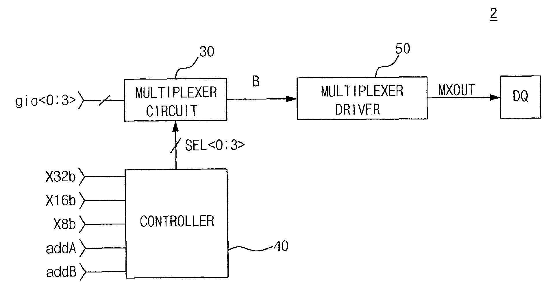
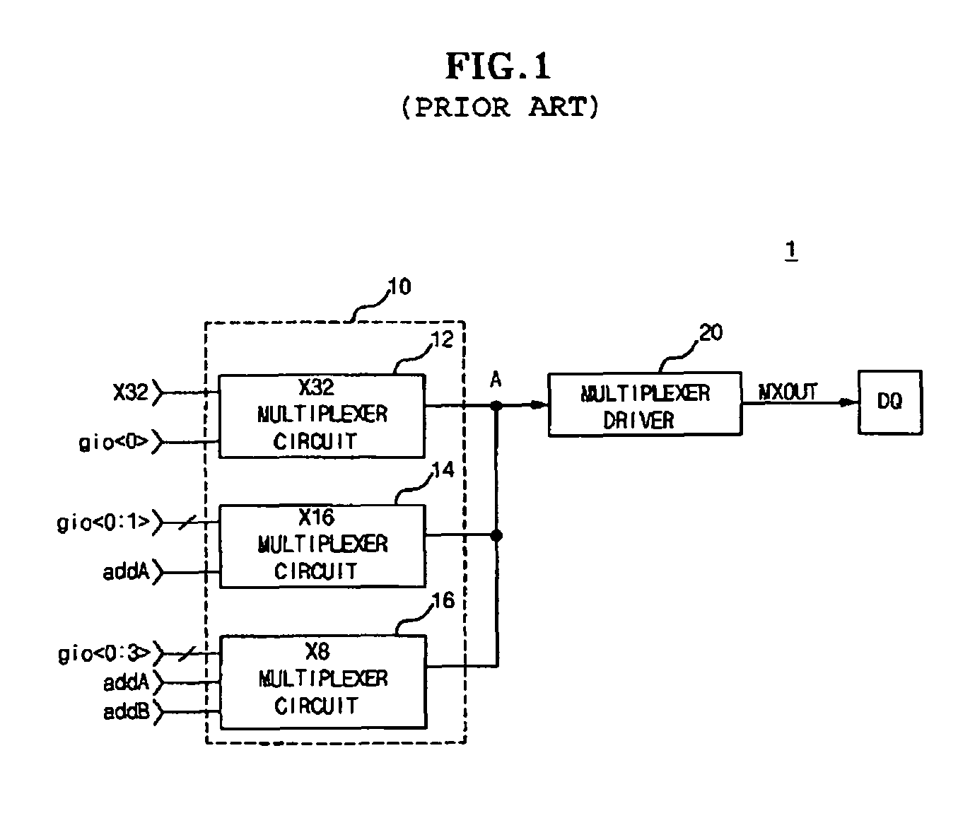
[0039]FIG. 3 depicts a block view showing a data output circuit of a semiconductor memory device according to the present invention. It shows a structure to support operation modes X32, X16, and X8 by performing a multiplexing corresponding to four global input / output lines (gio). Therefore, it is preferable that eight data output circuits as in FIG. 3 are further included.

[0040]Referring to FIG. 3, the data output circuit 2 is includes a multiplexer circuit 30, a controller 40, and a multiplexer driver 50.

[0041]The multiplexer circuit 30 controls the output of the data signals of a global input / output lines (gio) by means of control signals (SEL).

[0042]The controller 40 generates the control signals (SEL) in response to operation mode signals X32, X16, and X8 and in response to data selection signals addA and addB.

[0043]The multiplexer driver 50 ...


PUM


Abstract

The present invention relates to a semiconductor memory, and more specifically, to a data output circuit capable of differentiating global data lines in accordance to an operation mode to output them to a data input / output pin. The present invention includes: a multiplexer selecting any one of a plurality of global input / output lines which can receive variable data bandwidth directed by control signals and which can output data carried on the selected global input / output line, and a controller generating the control signals in accordance to operation mode signals corresponding to a data bandwidth and address signals provided for selecting data and providing them to the multiplexer. Thereby, the present invention can realize an improved data read speed by reducing the loading of the global input / output line.

Description

CROSS-REFERENCE TO RELATED APPLICATIONS[0001]The present application claims priority to Korean patent application number 10-2006-0086448 filed on Sep. 7, 2006, which is incorporated herein by reference in its entirety.BACKGROUND OF THE INVENTION[0002]The present invention relates to a semiconductor memory device, and more specifically to a data output circuit differentiating global data lines according to an operation mode to output them to data input / output pins.[0003]In general, in the case of a semiconductor memory device such as DDR SDRAM, it includes thirty-two data input / output pins (DQ) and thirty-two global input / output lines gin to support (X32, X16, and X8) data width options.[0004]Herein, an operation mode X32 uses thirty-two data input / output pins (DQ), an operation mode X16 uses sixteen data input / output pins (DQ), and an operation mode X8 uses eight data input / output pins (DQ).[0005]Accordingly, when data is read in the semiconductor memory device, an assignment of the...

Claims


Application Information

Patent Timeline
Patent Type & Authority Patents(United States)
IPC IPC(8): G11C7/10
CPCG11C7/1012G11C7/1048G11C7/1051G11C11/4093G11C7/1069G11C11/4097G11C7/18G11C7/10
Inventor KO, BOK RIM
Owner SK HYNIX INC
Why Eureka
Try Eureka