Method and apparatus for increasing data read speed in a semiconductor memory device

a technology of semiconductor memory and data read speed, applied in the direction of information storage, static storage, digital storage, etc., can solve the problem of increasing power consumption, and achieve the effect of increasing data read speed and reducing power consumption in data read operation

Inactive Publication Date: 2005-02-17
SAMSUNG ELECTRONICS CO LTD
View PDF5 Cites 1 Cited by
  • Summary
  • Abstract
  • Description
  • Claims
  • Application Information

AI Technical Summary

Benefits of technology

[0011] According to an exemplary embodiment of the present invention, a method for increasing data read speed and decreasing power consumption in data read operation of a semiconductor memory device comprising: applying a first internal power voltage to an input / output sense amplifier; and applying a second internal power voltage to a plurality of circuit components excluding the input / output sense amplifier.

Problems solved by technology

However, the method of increasing the power voltage supplied to all circuit components on the data read path increases the operation current of the semiconductor memory.
The aforementioned three circuit components draw an increased amount of current if the applied voltage is increased and thereby increase power consumption.

Method used


Image

  • Method and apparatus for increasing data read speed in a semiconductor memory device
  • Method and apparatus for increasing data read speed in a semiconductor memory device
  • Method and apparatus for increasing data read speed in a semiconductor memory device

Examples


Embodiment Construction

[0018] The exemplary embodiments of the present invention will now be described more fully hereinafter with reference to the accompanying drawings. This invention may, however, be embodied in different forms and should not be construed as limited to the embodiments set forth herein. Rather, these embodiments are provided so that this disclosure will be thorough and complete, and will fully convey the scope of the invention to those skilled in the art.

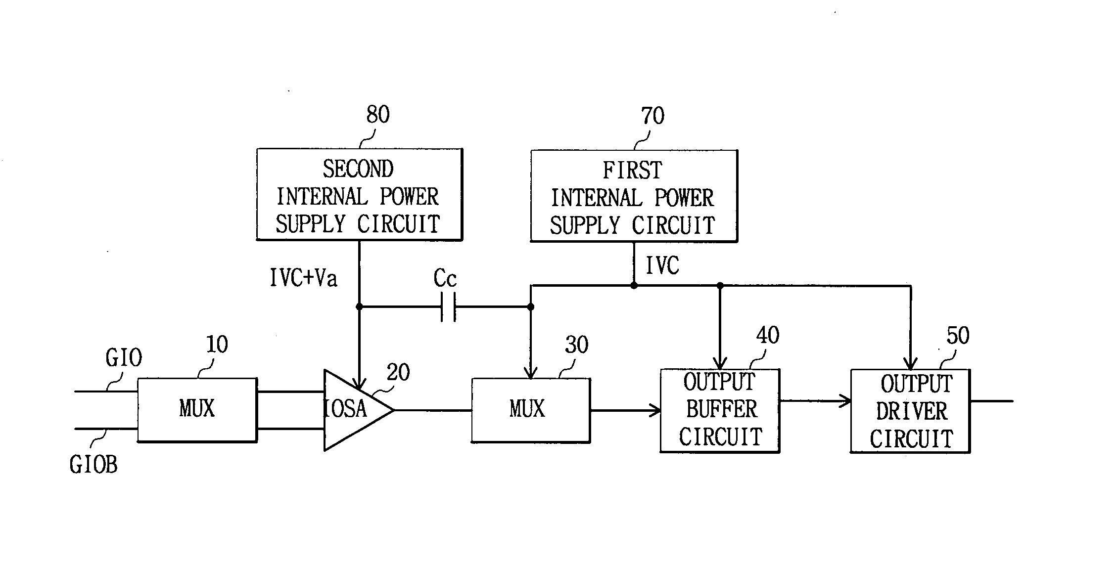
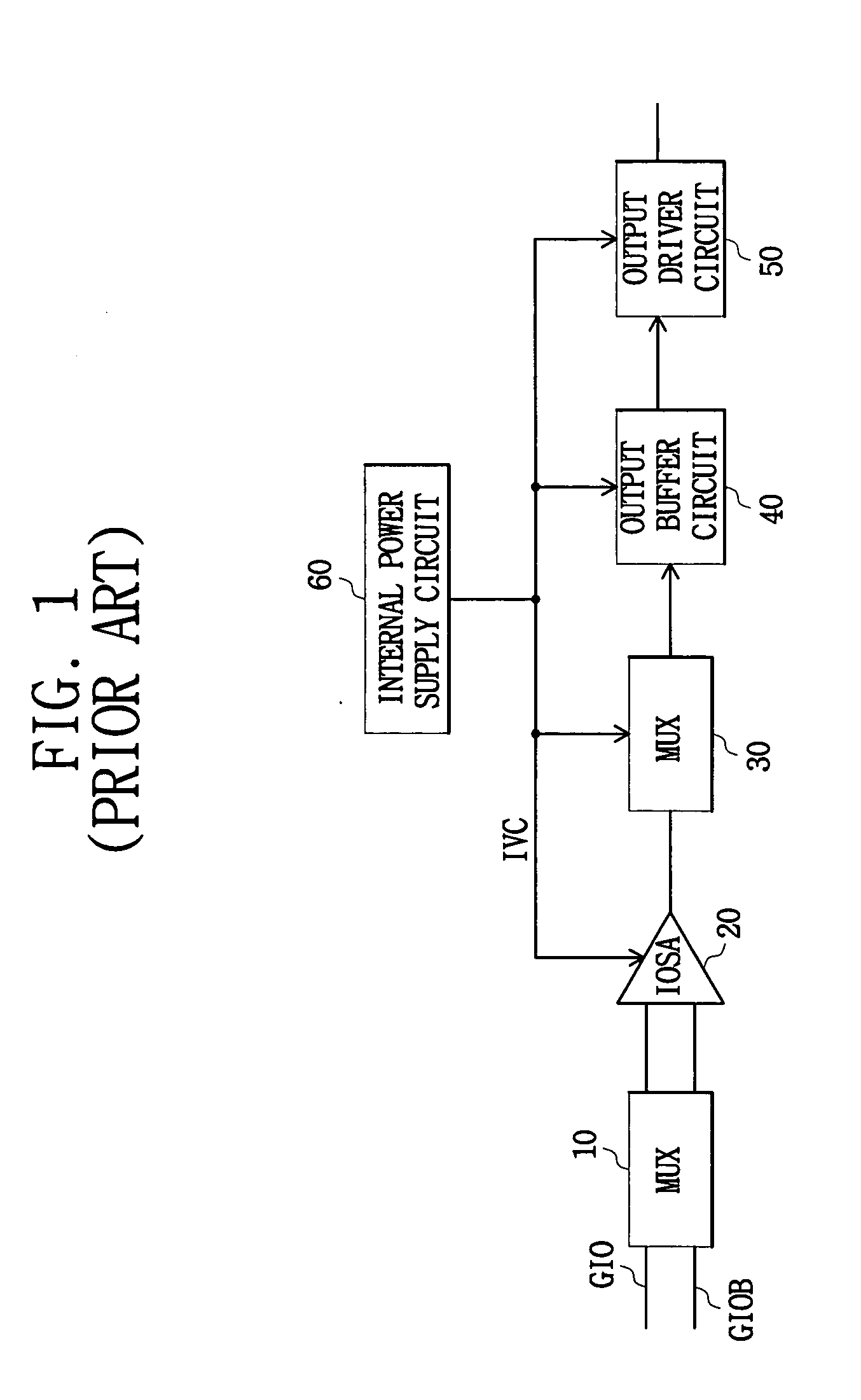
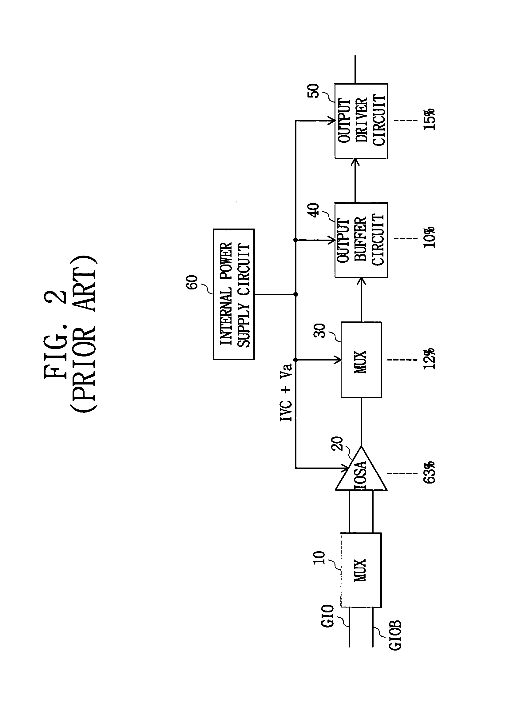
[0019]FIG. 3 is a block diagram illustrating a data read path of a memory cell in a semiconductor memory device according to a preferred embodiment of the present invention.

[0020] Referring to FIG. 3, a data read path of a semiconductor memory device according to an embodiment of the present invention includes a first MUX 10, an input / output sense amplifier (hereinafter, IOSA) 20, a second MUX 30, an output buffer circuit 40, an output driver circuit 50, a first internal power supply circuit 70, a second internal power supply circuit ...


PUM


Abstract

A semiconductor memory device having a data read path maintains a higher power voltage supplied to an input/output sense amplifier in the input/output path, through which data passes during a data read operation, than the voltage supplied to other circuit components in the data read path, thereby achieving a high data read speed.

Description

CROSS-REFERENCE TO RELATED APPLICATION [0001] This application claims the benefit of Korean Patent Application No. 2003-55898, filed Aug. 12, 2003, the disclosure of which is incorporated herein by reference in its entirety. BACKGROUND [0002] 1. Technical Field [0003] The present invention relates to a semiconductor memory device and, more particularly, to a data read path that increases data read speed and lowers power consumption in the semiconductor memory device. [0004] 2. Discussion of the Related Art [0005]FIG. 1 is a block diagram illustrating a data read path of a memory cell in a conventional semiconductor memory device. In the conventional semiconductor memory device of FIG. 1, the same internal power voltage (hereinafter, referred to as “IVC”) is supplied to the whole data read path, which amplifies data of a memory cell (not shown) and reads it. The data read path includes a first MUX 10, an input / output sense amplifier (hereinafter, referred to as “IOSA”) 20, a second M...

Claims


Application Information

Patent Timeline
Patent Type & Authority Applications(United States)
IPC IPC(8): G11C11/4091G11C5/14G11C7/10
CPCG11C5/14G11C7/1069G11C7/1051G11C7/1012G11C11/4091
Inventor LEE, CHAN-YONGLEE, JUNG-HWA
Owner SAMSUNG ELECTRONICS CO LTD
Why Eureka
Try Eureka