CDR control architecture for robust low-latency exit from the power-saving mode of an embedded CDR in a programmable integrated circuit device

a programmable integrated circuit and control architecture technology, applied in the direction of digital transmission, synchronisation signal speed/phase control, instruments, etc., can solve the problems of increasing unreliability of the approach and not being feasible for the vast majority of clock data recovery (cdr) implementations, so as to avoid unnecessary delay in the detection of the synchronization signal and minimize drift

Active Publication Date: 2012-10-16
ALTERA CORP
View PDF13 Cites 1 Cited by
  • Summary
  • Abstract
  • Description
  • Claims
  • Application Information

AI Technical Summary

Benefits of technology

[0007]Rather than relying on analog signal detection to indicate to CDR circuitry that an associated receiver has exited from an electrical idle period, in accordance with the present invention CDR circuitry of a high-speed serial interface on a programmable integrated circuit device toggles, during the electrical idle period of the receiver of the interface, between its “lock-to-reference” (“LTR”) state and its normal “lock-to-data” (“LTD”) state. Whenever during this toggling mode the CDR circuitry toggles to the LTD state, it remains in that state for a predetermined interval and then returns to the LTR state, unless, while it is in the LTD state, it receives a signal from elsewhere in the receiver that data have been received and byte synchronization, which is a digital process, has occurred. The predetermined toggling interval preferably is long enough to obtain an LTR lock to minimize drift in the frequency of a clock recovered before the receiver entered the electrical idle period, but short enough to avoid unnecessary delay in detection of the synchronization signal. Preferably, this interval is programmable by the user within limits determined by the characterization of the programmable logic device.

Problems solved by technology

This approach has been shown to be increasingly unreliable, especially in the context of emerging protocols such as PCI Express Gen 2 in which the receiver sensitivity at 5 Gb / s is 120 mV and the idle detection threshold is 175 mV.
However, the corresponding mechanisms specified to infer electrical idle exit, such as the detection of a recurring low frequency pattern of successive K28.7 symbols prior to LOs exit, are designed to be implemented in the analog domain and necessitate a bit lock time of less than 32 ns, which may not be feasible for the vast majority of clock data recovery (CDR) implementations.

Method used


Image

  • CDR control architecture for robust low-latency exit from the power-saving mode of an embedded CDR in a programmable integrated circuit device
  • CDR control architecture for robust low-latency exit from the power-saving mode of an embedded CDR in a programmable integrated circuit device
  • CDR control architecture for robust low-latency exit from the power-saving mode of an embedded CDR in a programmable integrated circuit device

Examples


Embodiment Construction

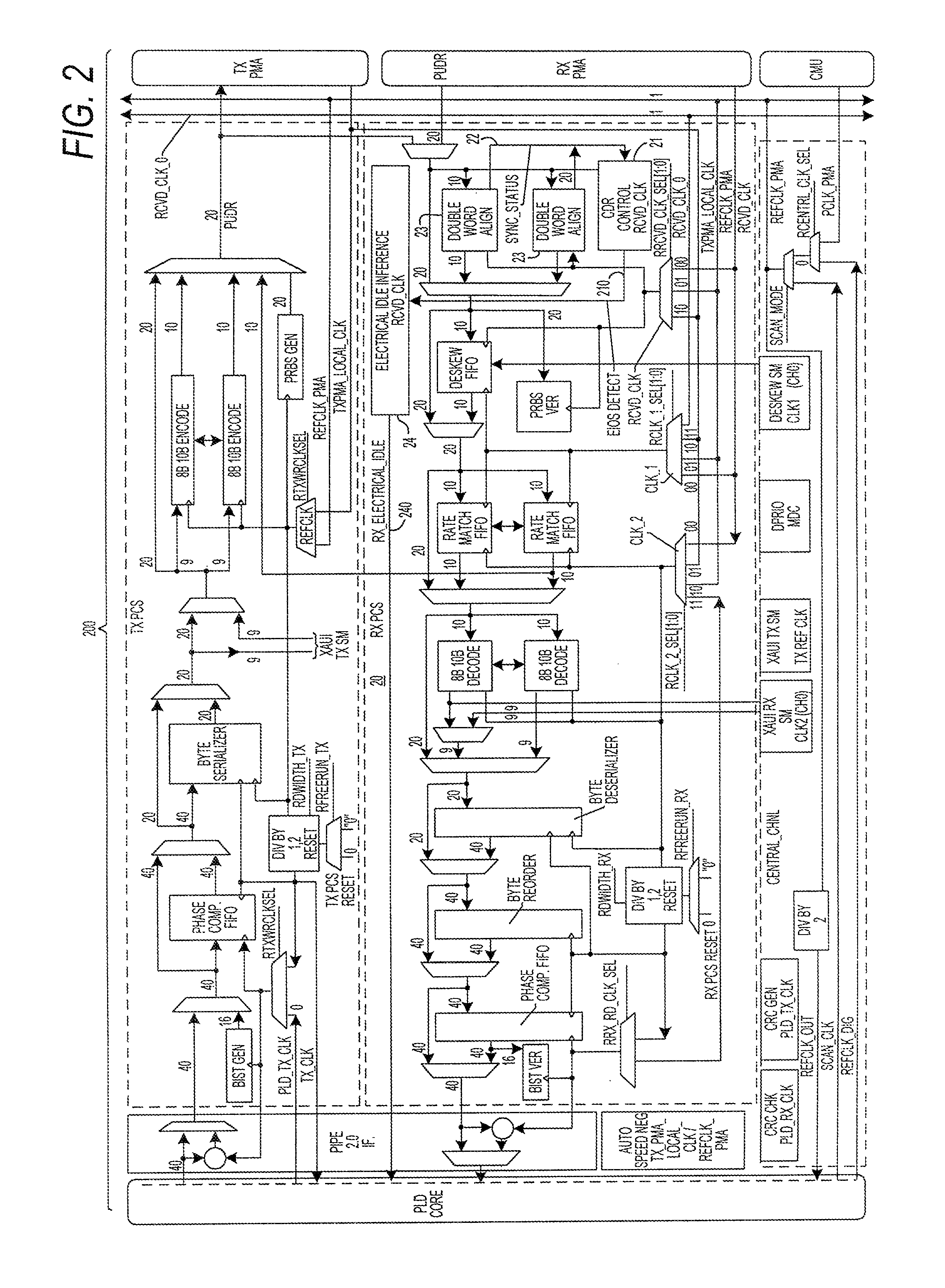
[0014]In a common implementation, a high-speed serial transceiver is divided into a physical medium attachment (PMA) portion or module which communicates with outside devices, and a physical coding sublayer (PCS) portion or module which performs serial processing of data, for transmission to, or that is received from, those outside devices. CDR circuitry typically is part of the PCS.

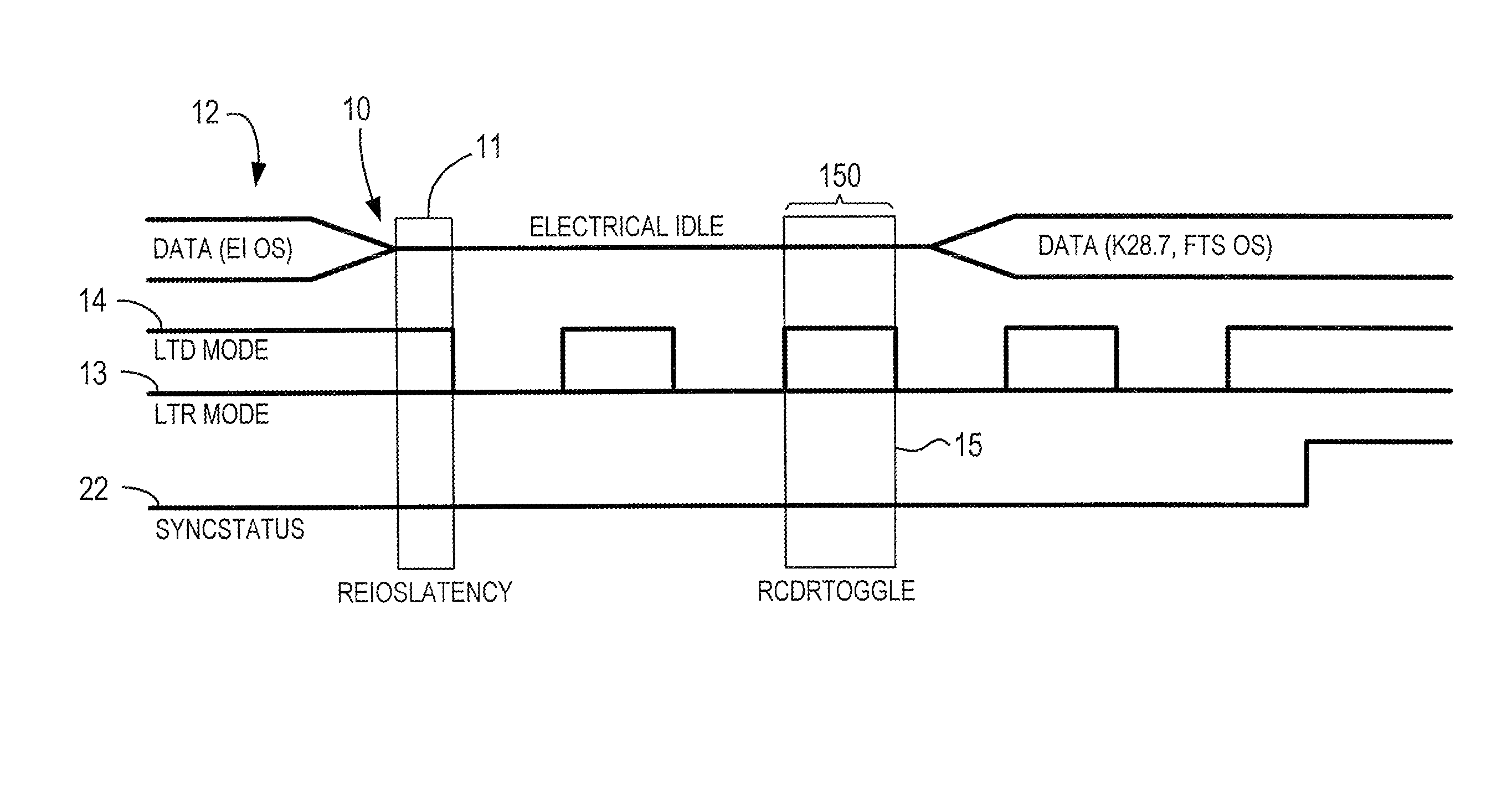
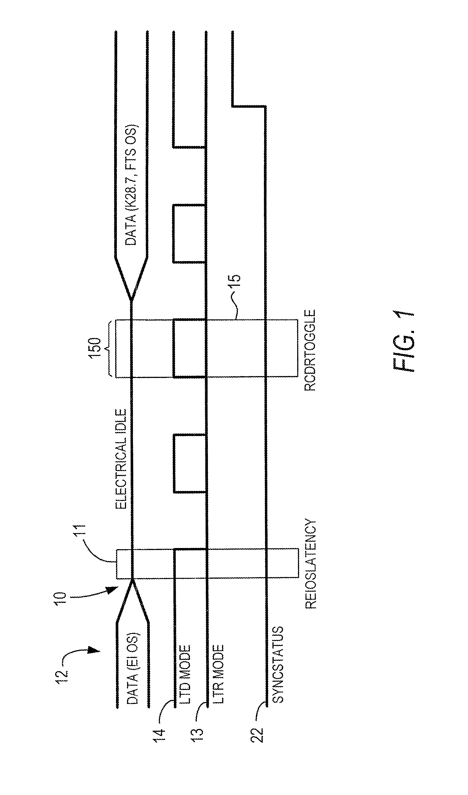
[0015]It is known to provide CDR circuitry with (a) a Lock-to-Data (LTD) state which is the normal operational state of the CDR circuitry, in which the circuitry locks to, and recovers the clock from, incoming data, and (b) a Lock-to-Reference (LTR) state which is a state in which the circuitry is not trying to perform its LTD function, but is locked to its own reference clock to minimize drifting to avoid providing a false output. The digital CDR control architecture of the present invention preferably drives the LTR and LTD outputs to the Physical Medium Attachment (PMA) in such a way as to align the l...


PUM


Abstract

Clock data recovery (CDR) circuitry of a high-speed serial interface on a programmable integrated circuit device toggles, during the electrical idle period of the receiver of the interface, between its “lock-to-reference” (“LTR”) state and its normal “lock-to-data” (“LTD”) state. Whenever during this toggling mode the CDR circuitry toggles to the LTD state, it remains in that state for a predetermined interval and then returns to the LTR state, unless, while it is in the LTD state, it receives a signal from elsewhere in the receiver that data have been received and byte synchronization has occurred. The predetermined toggling interval preferably is long enough to obtain an LTR lock to minimize frequency drift, but short enough to avoid unnecessary delay in detection of the synchronization signal. Preferably, this interval is programmable by the user within limits determined by the characterization of the programmable device. Unreliable analog signal detection is thereby avoided.

Description

CROSS REFERENCE TO RELATED APPLICATION[0001]This is a continuation of commonly-assigned U.S. patent application Ser. No. 11 / 857,141, filed Sep. 18, 2007 and now U.S. Pat. No. 7,925,913, which claims the benefit of commonly-assigned U.S. Provisional Patent Application No. 60 / 916,056, filed May 4, 2007, each of which is hereby incorporated by reference herein in its respective entirety.BACKGROUND OF THE INVENTION[0002]This invention relates to electrical idle exit detection for clock-data recovery circuitry in a high-speed serial interface of a programmable integrated circuit device such as a programmable logic device.[0003]As it becomes more important to minimize power consumption in programmable logic devices with embedded high-speed serial interfaces, it is desirable to use power-saving modes provided by the serial protocols supported by the devices to the fullest extent possible. One such mode is the PCI Express L0 Standby (L0s) low-power mode in which a link is placed in electric...

Claims


Application Information

Patent Timeline
Patent Type & Authority Patents(United States)
IPC IPC(8): G06F1/00H04L7/00H04L7/02
CPCG06F13/385H04L7/0083H04L7/033H04L7/10G06F13/4295Y02D10/00
Inventor VIJAYARAGHAVAN, DIVYAZHENG, MICHAEL MENGHUICHAN, LANA MAYLEE, CHONG H.
Owner ALTERA CORP
Why Eureka
Try Eureka