System and method of transistor switch biasing in a high power semiconductor switch

a high-power semiconductor and transistor switch technology, applied in electronic switching, pulse automatic control, pulse technique, etc., can solve the problems of consuming extra dc power, affecting the reliability and robustness of the circuit, and creating noise, spurious tones, and spurious spectral emission

Active Publication Date: 2012-12-11
SKYWORKS SOLUTIONS INC +1
View PDF6 Cites 34 Cited by
  • Summary
  • Abstract
  • Description
  • Claims
  • Application Information

AI Technical Summary

Problems solved by technology

Some of the drawbacks of the series shunt switch 100 of FIG. 1A are that it requires oscillators, charge pump circuitry, positive and negative voltage regulators, supply filtering including a negative supply filter which usually occupies a much larger area than a positive supply filter, and a pseudo-random bit sequence (PRBS) generator.
The additional components can create noise, spurious tones, and spurious spectral emissions and tend to occupy a large percentage of IC (integrated chip) die area, and consume extra DC power.
Some of the drawbacks of the series-shunt switch 150 of FIG. 1B are that it often requires a DC-DC boost converter circuit (not shown), and requires that all terminals be blocked with an appropriately sized blocking capacitor in order to ensure flexible voltage settings.
Integrated DC blocking capacitor's take up significant IC die area and may easily be damaged during ESD (ElectroStatic Discharge) events hampering the reliability and robustness of the circuit.
Use of off chip capacitors also occupies a significant board area and can add significant cost.

Method used


Image

  • System and method of transistor switch biasing in a high power semiconductor switch
  • System and method of transistor switch biasing in a high power semiconductor switch
  • System and method of transistor switch biasing in a high power semiconductor switch

Examples


Embodiment Construction

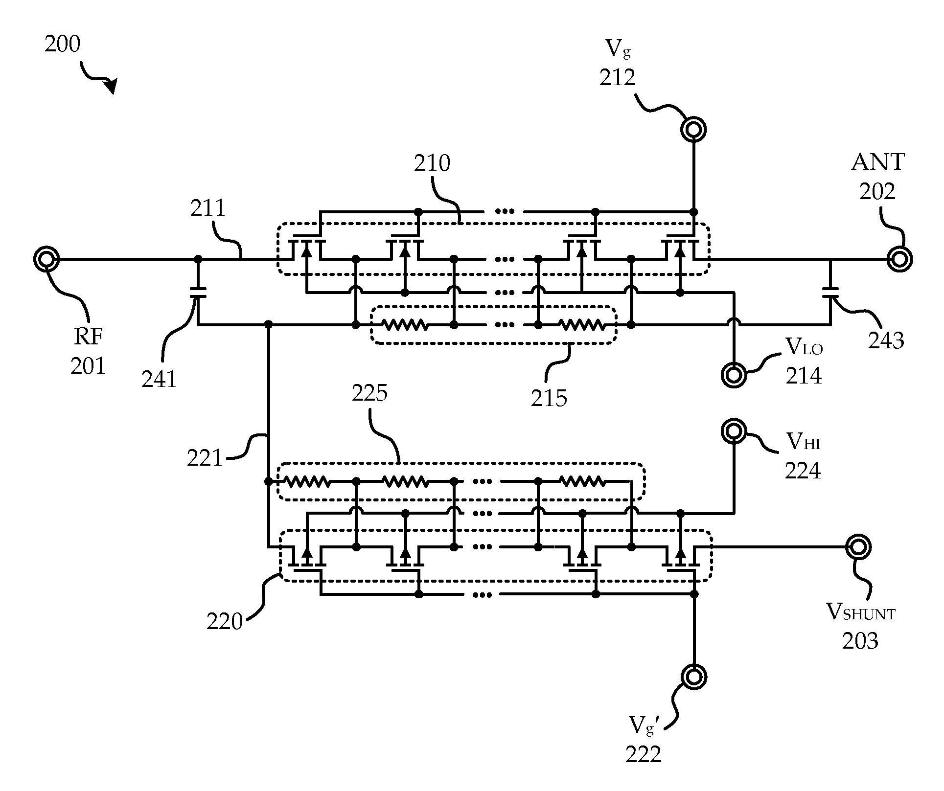
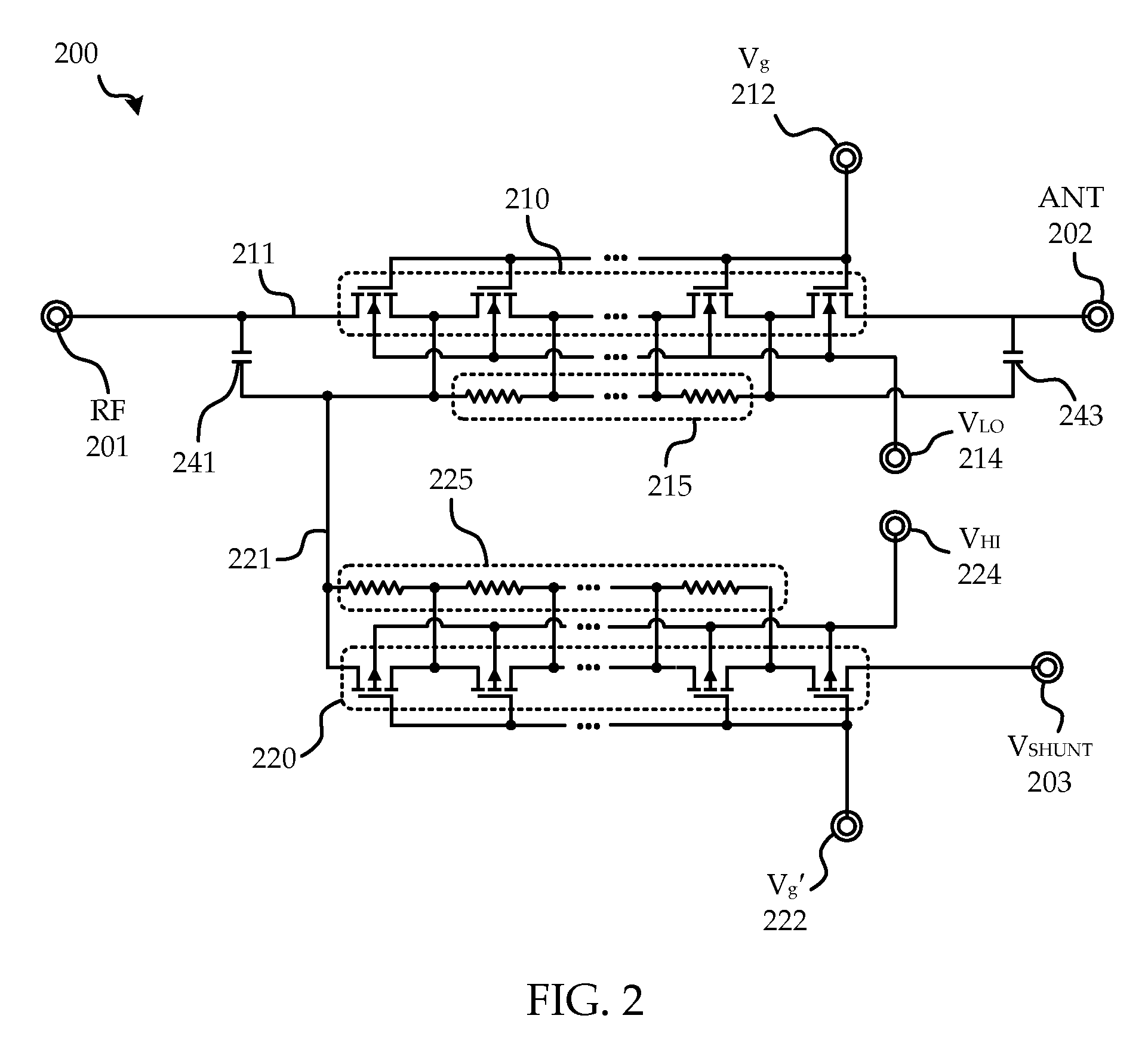
[0024]Referring to FIG. 2, a series-shunt switch 200 in accordance with a first embodiment of the invention will now be discussed in terms of its structure.

[0025]An RF terminal 201 is coupled along a series path 211 through a series n-FET group switch 210 to an antenna 202, and is connected along a shunt path 221 through a first blocking capacitor 241 in series with a shunt p-FET group switch 220 to an AC ground or shunt terminal 203. The series n-FET group switch 210 is made up of a plurality of n-type FET transistors, while the shunt p-FET group switch 220 is made up of a plurality of p-type FET transistors. Each FET group switch 210, 220 is connected in series with the respective path from the RF terminal 201 to the antenna 202 or from the RF terminal 201 to the shunt terminal 203. Each FET group switch 210, 220 also has a respective associated group of source / drain resistors 215, 225. Each n-FET of the series n-FET group switch 210, except for the last n-FET on the RF end of the...


PUM


Abstract

A circuit and method are provided for switching in a semiconductor based high power switch. Complementary p-type based transistors are utilized along insertion loss insensitive paths allowing biasing voltages to alternate between supply and ground, allowing for negative voltage supplies and blocking capacitors to be dispensed with, while improving performance.

Description

FIELD OF THE INVENTION[0001]The invention relates to high power semiconductor switches, and more particularly to FET switch layouts and biasing thereof.BACKGROUND OF THE INVENTION[0002]In modern RF communication systems, a semiconductor-based transmit-receive switch is often the last / first component encountered by a transmitted / received signal before / after encountering an antenna.[0003]Many of the main advances in semiconductor-based transmit-receive switches have been with respect to isolation and insertion loss. Groups of FETs are arranged in the switch along with judiciously chosen resistors and capacitors to ensure low insertion loss along the signal path and high isolation from the off paths. One general approach utilizes, instead of a single FET switch along each alternative path, a group of FET switches in series. This general approach moreover does not simply turn the FETs on and off by utilizing only a voltage at the gate, but instead biases both the gate and the source / dra...

Claims


Application Information

Patent Timeline
Patent Type & Authority Patents(United States)
IPC IPC(8): H03L5/00
CPCH03K17/693H03K5/003H03K2217/0018
Inventor LAM, LUI RAYFUH, HANCHING
Owner SKYWORKS SOLUTIONS INC
Why Eureka
Try Eureka