Package for electronic component, piezoelectric device and manufacturing method thereof

a piezoelectric device and electronic component technology, applied in the direction of generator/motor, fluid pressure measurement, instruments, etc., can solve the problems of low or deteriorating frequency characteristics of piezoelectric resonator elements, difficult to promote sealing, and insufficient heat to the sealant, so as to improve the manufacturing efficiency of the piezoelectric device

Active Publication Date: 2012-12-18
138 EAST LCD ADVANCEMENTS LTD
View PDF12 Cites 10 Cited by
  • Summary
  • Abstract
  • Description
  • Claims
  • Application Information

AI Technical Summary

Benefits of technology

[0010]When the electronic component is sealed by the package for an electronic component, the sphere sealant made of metal is often provided in the sealing hole and is melted so as to cover the sealing hole. According to the structure above, the interior wall of the sealing hole formed in at least one of the first substrate and the second substrate includes a curved surface extending in the directions of penetration and inner periphery of the sealing hole. Therefore, when the solid sealant is provided in the sealing hole, the portion where the surface of the sphere sealant contacts with or closes to the interior wall of the sealant can be widely ensured. Accordingly, when the sealant is melted for sealing the sealing hole, heat can be well conducted to the sealant through the interior wall surface of the sealing hole. Further, since the melted sealant easily wets and covers the interior wall surface of the sealing hole, sealing defects are suppressed. As a result, a piezoelectric device having stable oscillation characteristics and high reliability can be provided.
[0024]According to the structure, when the sphere and solid sealant is provided in the sealing hole, the opening communicating with the opening at the exterior side and the opening at the interior space side is off-center from the center of the opening at the exterior side. Therefore, a space can be easily ensured between the interior wall of the sealing hole and the sealant, so that the vacuuming time in the hole sealing step, in which the electronic component is airtightly sealed in the interior space, is shortened and manufacturing efficiency of the piezoelectric device can be improved.

Problems solved by technology

However, the related-art package structure, in which a package and a lid are bonded with low-melting point glass or by seam welding, may lower or deteriorate frequency characteristics of piezoelectric resonator elements due to outer gas, high heat or the like generated in the seam welding.
When the sealant is melted for sealing the sealing hole, heat is not efficiently conducted to the sealant.
Therefore, it is hard to promote melting of the sealant, and also the melted sealant is hard to wet and cover the interior surface of the sealing hole.
Accordingly, it is hard to ensure airtight properties of the sealing, and reliability of the piezoelectric device may be decreased by malfunction of the piezoelectric resonator element due to sealing defects and influence of external factors.

Method used


Image

  • Package for electronic component, piezoelectric device and manufacturing method thereof
  • Package for electronic component, piezoelectric device and manufacturing method thereof
  • Package for electronic component, piezoelectric device and manufacturing method thereof

Examples


first embodiment

[0036

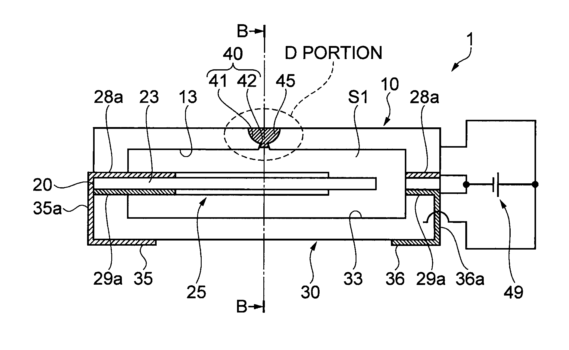
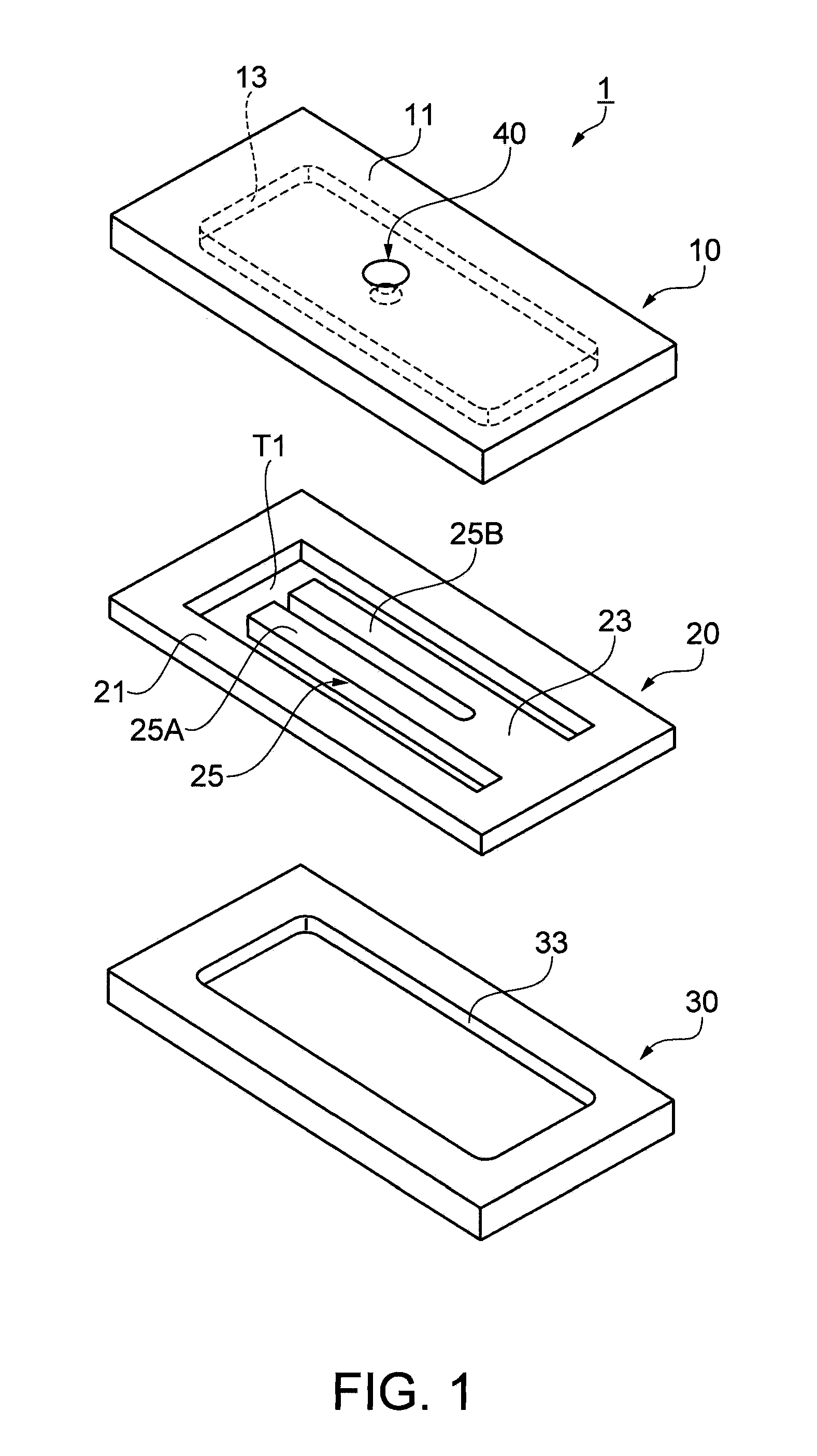
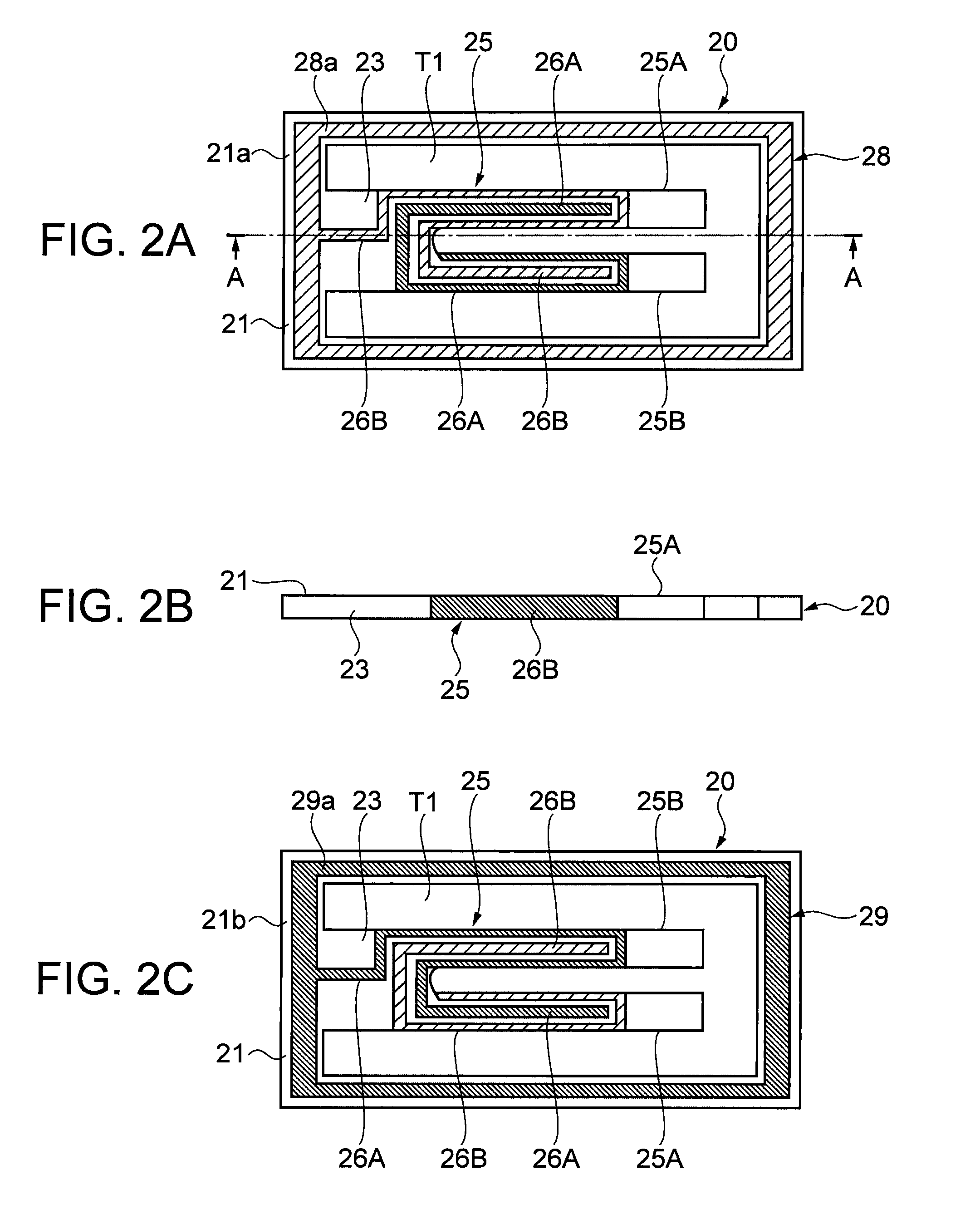
[0037]FIGS. 1 to 3 show an embodiment in which a piezoelectric resonator serving as a piezoelectric device is realized as a crystal resonator. FIG. 1 is an exploded perspective view schematically showing the piezoelectric resonator. FIGS. 2A, 2B, and 2C are schematic views showing a resonator element substrate that a crystal resonator element serving as a piezoelectric resonator element is integrally formed with a frame. FIG. 2A is a plan view, FIG. 2B is a sectional view taken along line A-A of FIG. 2A, and FIG. 2C is a bottom view of the resonator element substrate. FIG. 3 is a sectional view schematically showing a cross-sectional structure of the crystal resonator and the state where anodic oxidation is performed. FIG. 3 also shows a sectional view of the crystal resonator shown in FIG. 1 taken along line of A-A of FIG. 2.

[0038]Referring to FIG. 1, a crystal resonator 1 is composed of a lid substrate 10 serving as a first substrate, a resonator element substrate 20, and a b...

first modification

[0093

[0094]In the embodiment above, the center of the opening at the exterior side is the same as the center of the openings 42a and 42b at the interior space side in the sealing hole 40 that includes the exterior side concave 41 and the interior space side concave 42 in communication with each other at the opening 42a formed at the concave bottom of the exterior side concave 41. The exterior side concave 42 is a hemisphere including the opening at the exterior side surface 11 of the lid substrate 10. The interior space side concave 42 includes the opening 42b at the interior space side. Not only the structure above, but also the structure can be employed that the center of the opening of the exterior side concave is off-center from the center of the opening of the interior space side concave. This makes it possible to increase efficiency in vacuuming in the hole sealing step. FIGS. 6A and 6B are schematic views showing the modification of sealing the hole in the lid substrate. FIG....

second modification

[0098

[0099]In the sealing holes 40 and 80 of the lid substrates 10 and 70 according to the embodiment and the first modification above, the exterior side concaves 41 and 81 and the interior space side concaves 42 and 82 in communication with each other are a circle when the sealing holes are plan-viewed. Not only the structure above, but also a structure can be employed that the upper side and the bottom side openings of the interior space side concave are an oval when the openings are plan-viewed. This makes it possible to increase efficiency in vacuuming in the hole sealing step. FIGS. 7A and 7B are schematic views showing the second modification of sealing the hole in the lid substrate. FIG. 7A is a partial plan view of the lid substrate when viewed from the exterior side. FIG. 7B is a partial sectional view taken along line F-F of FIG. 7A. Here, for convenience of the description, FIGS. 7A and 7B show the state where the sphere sealant 45a before melted is provided in a sealing ...


PUM

PropertyMeasurementUnit
areaaaaaaaaaaa
melting pointaaaaaaaaaa
structureaaaaaaaaaa

Abstract

A package for an electronic component includes a first substrate and a second substrate. In the package, an interior space capable of housing the electronic component is formed between the first substrate and the second substrate, a sealing hole communicating with the interior space and an exterior is formed in at least one of the first substrate and the second substrate, the interior space can be airtightly sealed by melting a solid sealant provided in the sealing hole, and an interior wall of the sealing hole has a curved surface extending in directions of penetration and inner periphery of the sealing hole.

Description

BACKGROUND[0001]1. Technical Field[0002]The present invention relates to a package for an electronic component including an interior space in which the electronic component is airtightly sealed, a piezoelectric device airtightly sealing a piezoelectric resonator element serving as the electronic component, and a manufacturing method of the piezoelectric device.[0003]2. Related Art[0004]Piezoelectric devices, such as crystal resonators, have been used in various information and communication devices, office automation (OA) equipment, and electronic apparatuses, such as consumer-electronics devices. Especially in recent years, significant progress in improving performance as well as downsizing and thinning of the electronic apparatuses and the like has been made. In order to respond to demands for smaller and thinner devices, surface-mounted piezoelectric devices suitably mounted on circuit boards have been widely used. In general, surface-mounted piezoelectric devices have a structur...

Claims


Application Information

Patent Timeline
Patent Type & Authority Patents(United States)
IPC IPC(8): H01L41/08H01L23/02H03H3/02H03H9/02
CPCG01L9/0022H03H9/1035H03H9/0595Y10T29/42H01L23/10H10N30/80
Inventor SAITA, HIROYASU
Owner 138 EAST LCD ADVANCEMENTS LTD
Why Eureka
Try Eureka