Detector system for transmission electron microscope

a transmission electron microscope and detector system technology, applied in the field of electron microscopy, can solve the problems of reducing the detector resolution, the limited field of view provided, and the time required to read out the array of pixels, so as to improve the quality of tem imaging

Active Publication Date: 2012-12-25
FBI
View PDF35 Cites 15 Cited by
  • Summary
  • Abstract
  • Description
  • Claims
  • Application Information

AI Technical Summary

Benefits of technology

[0011]An object of the invention is to improve the quality TEM imaging.
[0013]In one embodiment, artifacts that degrade the image acquired using cryo-or other low electron dose TEM can be reduced or eliminated by analyzing data obtained at different times during the image acquisition period to identify and eliminate image data corresponding to artifacts. For example, data taken at the beginning of an image acquisition period from fewer than all the pixels is used to determine when charging is complete, and only image data that is not affected by charging is collected. In another embodiment, image data is analyzed to determine whether the sample is bubbling, and the image-forming period is ended at the onset of bubbling.

Problems solved by technology

The extra step of converting the electrons to light reduces the detector resolution because the light from the phosphor spreads before it reaches the CCD detector.
Another disadvantage of the CCD detector is the time required to read out the array of pixels, and the limited field of view provided.
Biological samples, which contain a large amount of water would quickly degrade in a high vacuum environment.
Images from a cryo-TEM, however, are degraded by various processes that occur during the observation.
For example, the impact of high energy electrons in the beam heats the thin sample which, and after a short period of observation can cause bubbles in the sample.
Another problem with cryo-TEM is that samples accumulate a static electric charge at the beginning of imaging, which produces significant streaking in the corners of the image.
Both these methods have the undesirable effect of reducing the time that the electron beam is producing useful information, since the pre-illumination begins to heat the sample, but does not produce useful image data.

Method used


Image

  • Detector system for transmission electron microscope
  • Detector system for transmission electron microscope
  • Detector system for transmission electron microscope

Examples


Embodiment Construction

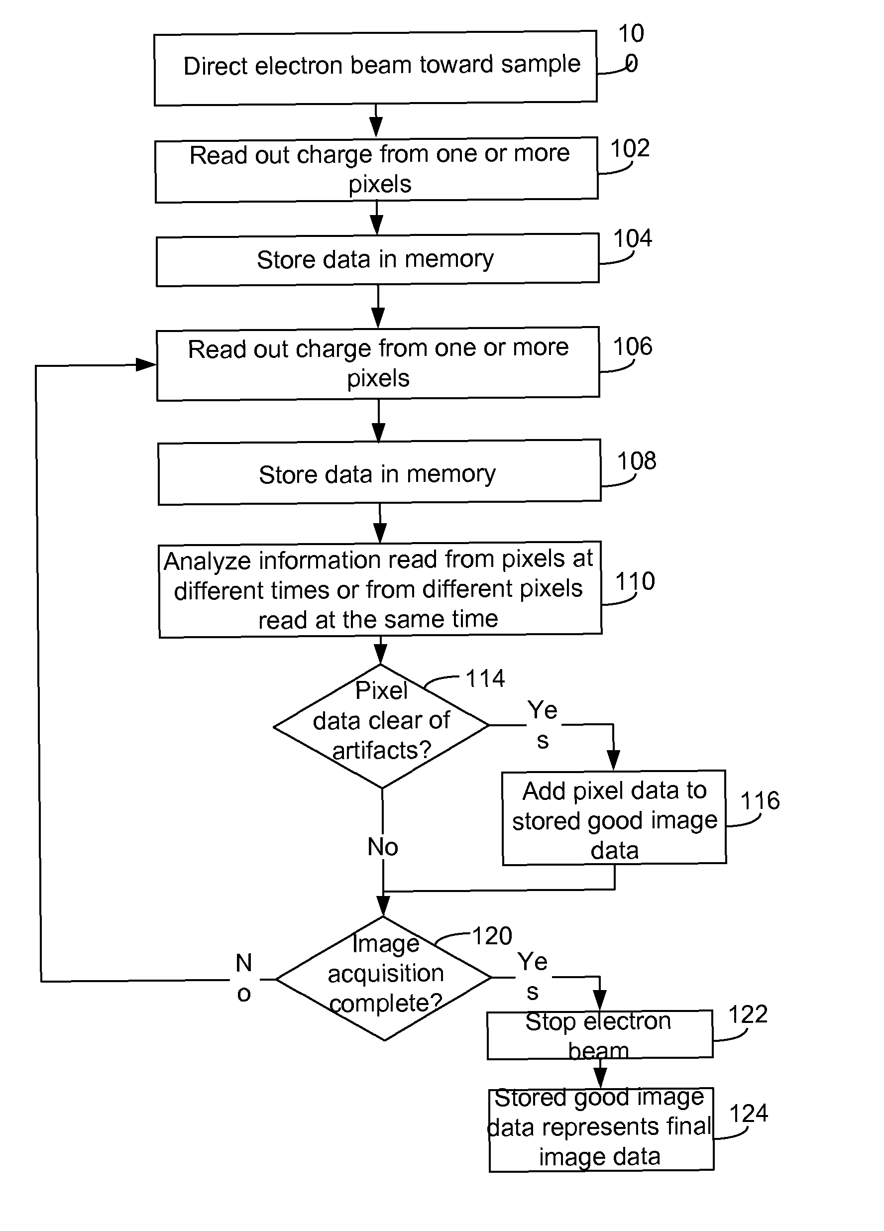
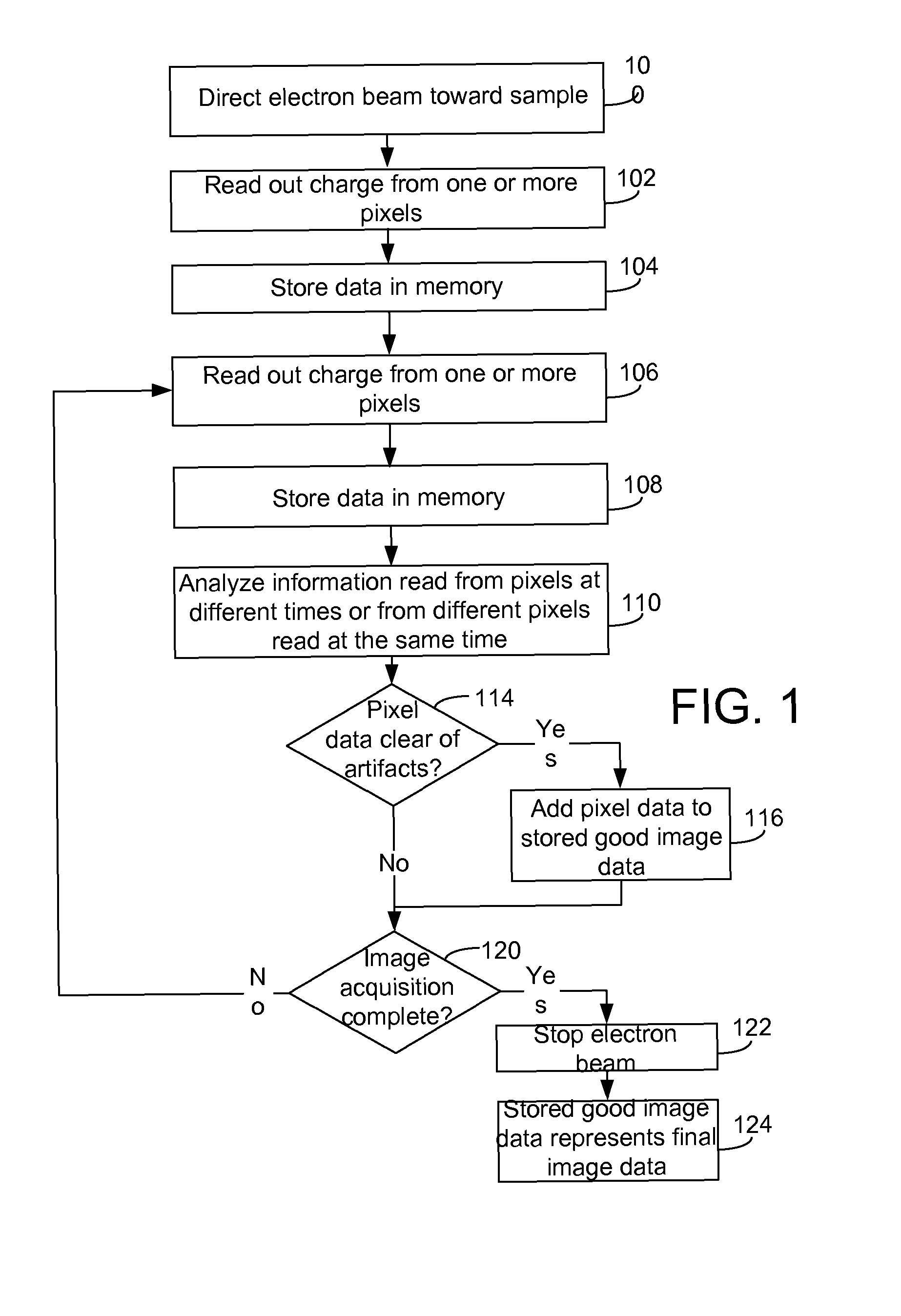
[0022]Imaging artifacts that occur in images from an electron microscope may render the image less useful. Many artifacts change over time and can be identified and eliminated by comparing image data taken at different times during an image acquisition period. Some artifacts may also be identified by comparing data representing different regions of a single frame. “Frame” as used herein, means a group of pixel data read out in a single read-out period, that is, a group of pixel data read out at essentially the same time. The frame may include data from all pixels or from fewer than all pixels. In a preferred embodiment of the present invention, image data is read from the detector at multiple times while the image is being acquired. That is, a single image can be formed using data from multiple frames. The image data from the different times, or from different parts of the image at the same time, can be compared to determine the presence of artifacts, and such artifacts can be elimi...


PUM

PropertyMeasurementUnit
thickaaaaaaaaaa
thickaaaaaaaaaa
frequencyaaaaaaaaaa

Abstract

In a transmission electron microscope detector system, image data is read out from the pixels and analyzed during an image acquisition period. The image acquisition process is modified depending on the results of the analysis. For example, the analyses may indicate the inclusion in the data of an image artifact, such as charging or bubbling, and data including the artifact may be eliminated form the final image. CMOS detectors provide for selective read out of pixels at high data rates, allowing for real-time adaptive imaging.

Description

[0001]This application claims priority from U.S. Provisional Patent Application 61 / 376,596, filed Aug. 24, 2010, which is hereby incorporated by reference.TECHNICAL FIELD OF THE INVENTION[0002]The present invention relates to electron microscopy, and in particular, to a detector system for use with electron microscopy.BACKGROUND OF THE INVENTION[0003]A transmission electron microscope (TEM) transmits an electron beam through a thin sample and detects changes in the electron beam caused by interactions between the electrons and the sample. The electrons are typically accelerated to energies of between 80 and 300 keV. The acceleration is preferably done by maintaining the electron source at a high voltage and accelerating the electrons toward a sample at ground potential. Deflectors, lenses, and aberration correctors may manipulate the beam to irradiate the sample. The sample is sufficiently thin to be partially transparent to the electrons.[0004]Because the transparency to electrons ...

Claims


Application Information

Patent Timeline
Patent Type & Authority Patents(United States)
IPC IPC(8): H01J37/26G01N23/00G21K7/00
CPCH01J37/222H01J37/26H01J37/265H01J2237/2446
Inventor LUECKEN, UWESCHOENMAKERS, REMCOSCHUURMANS, FRANK JEROEN PIETER
Owner FBI
Why Eureka
Try Eureka