Top-side cooled semiconductor package with stacked interconnection plates and method

a technology of interconnection plates and semiconductor packages, applied in the field of physical level packaging of semiconductor dies, can solve the problems of package footprint, non-conformity of external geometrical connections, packaging process, etc., and achieve the effect of adding effective top-side cooling to the semiconductor package and low thermal resistan

Active Publication Date: 2013-01-15
ALPHA & OMEGA SEMICON INC
View PDF4 Cites 25 Cited by
  • Summary
  • Abstract
  • Description
  • Claims
  • Application Information

AI Technical Summary

Benefits of technology

[0029]As a refinement, the periphery of the top surface of at least one stacked interconnection plate is partially etched. The partially etched periphery acts to strengthen the locking of the molding encapsulant to the top of the semiconductor package.
[0030]As another refinement, the top portion of at least one stacked interconnection plate includes a peripheral overhang above its correspondingly bonded intimate interconnection plates. The peripheral overhang allows for a maximized exposed top surface area for heat dissipation independent of otherwise areal constraints applicable to the selected number of intimate interconnection plates. The periphery of at least one stacked interconnection plate can be partially etched at its underside to create the peripheral overhang. Alternatively, at least one stacked interconnection plate can be three dimensionally formed to create the peripheral overhang.
[0031]As another refinement, each of the selected number of intimate interconnection plates can be shaped and sized, independently of the amount of exposed top surface of its corresponding stacked interconnection plate, to maximize its corresponding bonding areas on the semiconductor die thus reducing their associated spreading resistance.
[0032]As another refinement, at least one elevation-adaptive intimate interconnection plate can include numerous locking tabs placed in intermeshing relationship with a corresponding number of terminal leads nearby to minimize rotational creepage of the semiconductor die during a packaging process for the semiconductor package. Likewise, at least one stacked interconnection plate can include numerous locking tabs placed in intermeshing relationship with a corresponding number of terminal leads nearby to minimize rotational creepage of the semiconductor die during packaging as well.
[0036]In one embodiment, the circuit substrate can be made of a leadframe. Alternatively, the circuit substrate can be made of a laminated circuit having numerous thermal vias to increase bottom-side cooling.

Problems solved by technology

Thus, with the “DirectFET” approach, its external geometrical connections, or package footprint, are not configured to conform to an industry standard package pin out such as, for example, the SO-8 package footprint.
However, this packaging approach requires a flip-chip configuration that complicates the die packaging process.
This package is compatible with industry standard package pin outs, however this package does not achieve top side cooling.
However this package also does not achieve top side cooling.
U.S. Pat. No. 4,935,803 also does not achieve top side cooling.
All of them can only achieve limited effectiveness of top side cooling when heat-sinks are put in direct contact with the top of the package due to the limited amount of top metal exposed through the plastic encapsulation compound.
More specifically, as the number of top side die electrodes and / or the number of top side plate features of lower elevation (dimples, anchor holes, plane portions, valley portions, conductive bridges between fingers, windows) increase the available area for exposed top surface of each top side plate for heat dissipation correspondingly decreases causing further degradation of effectiveness of top side cooling.

Method used


Image

  • Top-side cooled semiconductor package with stacked interconnection plates and method
  • Top-side cooled semiconductor package with stacked interconnection plates and method
  • Top-side cooled semiconductor package with stacked interconnection plates and method

Examples


Embodiment Construction

[0070]The description above and below plus the drawings contained herein merely focus on one or more currently preferred embodiments of the present invention and also describe some exemplary optional features and / or alternative embodiments. The description and drawings are presented for the purpose of illustration and, as such, are not limitations of the present invention. Thus, those of ordinary skill in the art would readily recognize variations, modifications, and alternatives. Such variations, modifications and alternatives should be understood to be also within the scope of the present invention.

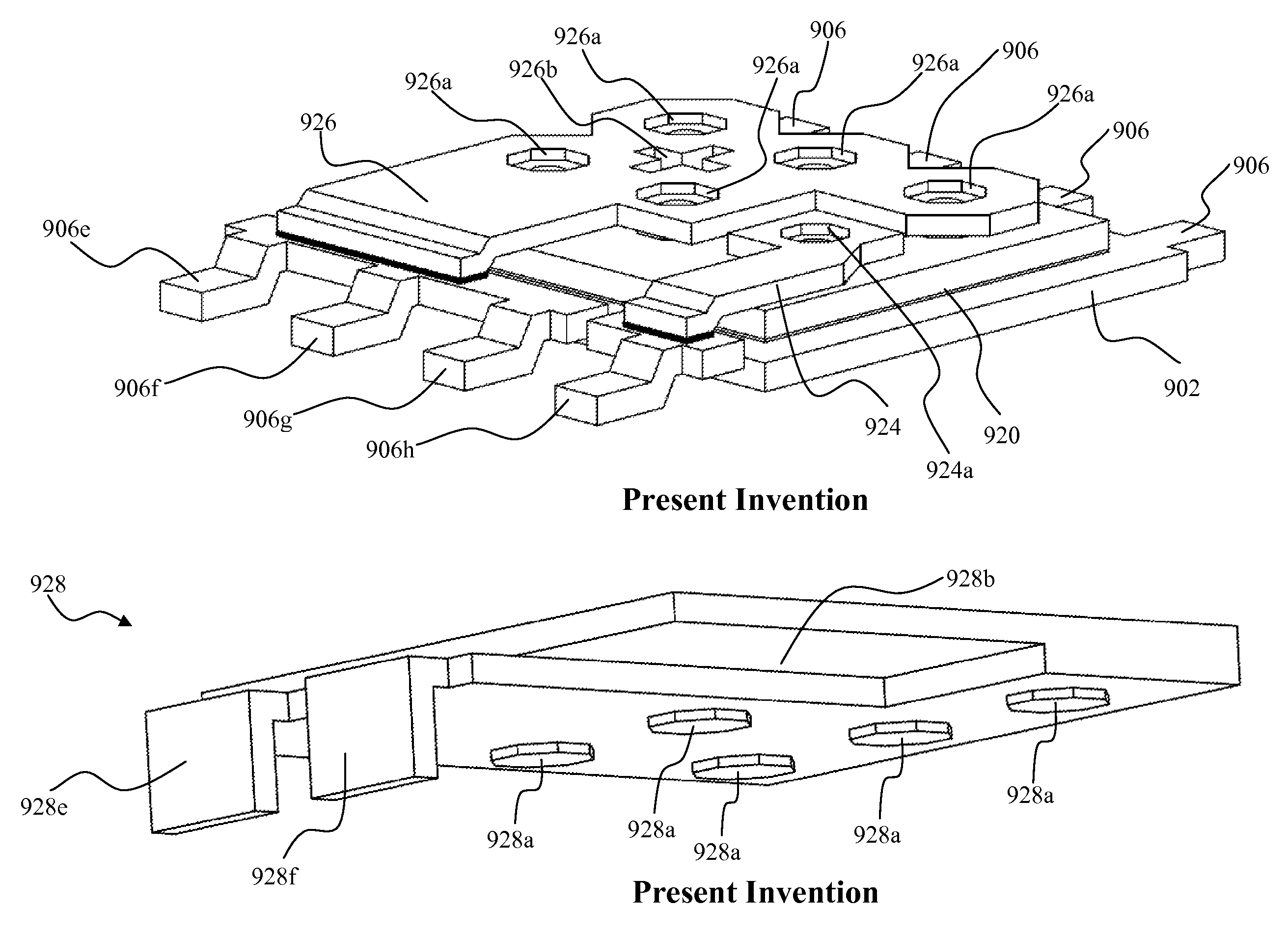
[0071]FIG. 5A and FIG. 5B illustrate a top-side cooled semiconductor package 500 having an intimate interconnection plate 526 and a stacked interconnection plate 528. FIG. 5B is a cross sectional view of FIG. 5A along a direction A-A. The top-side cooled semiconductor package 500 includes:[0072]A circuit substrate that is, in this illustrated example, a leadframe 502 having numerous ter...


PUM


Abstract

A top-side cooled semiconductor package with stacked interconnection plate is disclosed. The semiconductor package includes a circuit substrate with terminal leads, a semiconductor die atop the circuit substrate, a low thermal resistance intimate interconnection plate for bonding and interconnecting a top contact area of the semiconductor die with the circuit substrate, a low thermal resistance stacked interconnection plate atop the intimate interconnection plate for top-side cooling, a molding encapsulant for encapsulating the package except for exposing a top surface of the stacked interconnection plate to maintain effective top-side cooling. The top portion of the stacked interconnection plate can include a peripheral overhang above the intimate interconnection plate. The peripheral overhang allows for a maximized exposed top surface area for heat dissipation independent of otherwise areal constraints applicable to the intimate interconnection plate. The stacked interconnection plate can be partially etched or three dimensionally formed to create the peripheral overhang.

Description

CROSS REFERENCE TO RELATED APPLICATIONS[0001]This application is related to the following commonly assigned patent applications: U.S. application Ser. No. 11 / 799,467 entitled “SEMICONDUCTOR PACKAGE HAVING DIMPLED PLATE INTERCONNECTIONS” by Ming Sun et al, publication# US20070290336, hereafter referred to as U.S. application Ser. No. 11 / 799,467[0002]U.S. Patent Application Publication No. 20080087992 entitled “Semiconductor package having a bridged plate interconnection” by Shi Lei et al, hereafter referred to as US 20080087992[0003]Commonly assigned U.S. patent application Ser. No. 12 / 130,663 entitled “CONDUCTIVE CLIP FOR SEMICONDUCTOR DEVICE PACKAGE” by Shi Lei et al, hereafter referred to as U.S. application Ser. No. 12 / 130,663[0004]Commonly assigned U.S. patent application Ser. No. 12 / 237,953 entitled “Top Exposed Clip with Window Array” by Shi Lei et al, hereafter referred to as U.S. application Ser. No. 12 / 237,953whose content is incorporated herein by reference for any and all...

Claims


Application Information

Patent Timeline
Patent Type & Authority Patents(United States)
IPC IPC(8): H01L23/495
CPCH01L23/49524H01L23/49562H01L21/56H01L24/36H01L24/40H01L21/50H01L23/49568H01L2924/1305H01L2224/40249H01L2924/3011H01L2224/40247H01L2224/48247H01L2924/01013H01L2924/01027H01L2924/01033H01L2924/01078H01L2924/01079H01L2924/01082H01L2924/10329H01L2924/13055H01L2924/13091H01L2924/14H01L2924/30107H01L24/48H01L2924/01005H01L2924/01006H01L2924/01075H01L2224/37011H01L2224/32245H01L2224/73263H01L2924/00H01L2924/181H01L2224/40095H01L2224/4103H01L2224/40245H01L24/41H01L24/37H01L2924/00014H01L2224/84385H01L2224/84345H01L2224/29101H01L2224/83815H01L2224/84801H01L2224/8485H01L24/84H01L24/29H01L24/32H01L2924/00012H01L2224/45099H01L2224/45015H01L2924/207H01L2224/37099H01L2924/014H01L2924/0781H01L2224/73221
Inventor LIU, KAIHEBERT, FRANCOISSHI, LEI
Owner ALPHA & OMEGA SEMICON INC
Why Eureka
Try Eureka