Field effect device having a channel of nanofabric and methods of making same

a field effect device and carbon nanofabric technology, which is applied in the field of field effect devices having a channel of carbon nanofabric and a method of making the same, can solve the problems of 10 years to find a fabrication-only solution to the normally-fabricated nmos problem, the nmos devices were in the on state as fabricated, and the inability to fabricate only the problem of nmos devices, etc., to achieve the effect of modulating the conductivity of the channel region

Active Publication Date: 2013-01-29
NANTERO
View PDF121 Cites 7 Cited by
  • Summary
  • Abstract
  • Description
  • Claims
  • Application Information

AI Technical Summary

Problems solved by technology

A major problem was that NMOS devices were in the ON state as fabricated.
Positive ions both fixed and mobile, combined with the work function of the aluminum gate and p-substrate doping, plus defects in the Si / SiO2 interface made it impossible to find a fabrication-only solution to the fabricated normally-ON NMOS problem (it took well over 10 years to find a fabrication-only solution).
This method of operation could not meet the requirement of operating voltages in the zero to VDD range, with a positive threshold voltage.

Method used


Image

  • Field effect device having a channel of nanofabric and methods of making same
  • Field effect device having a channel of nanofabric and methods of making same
  • Field effect device having a channel of nanofabric and methods of making same

Examples


Embodiment Construction

Integrating SWNTs and CMOS Processes

[0052]Preferred embodiments of the present invention provide a fabrication solution to the controlled placement, patterning, and wiring of CNFET devices to enable the design of logic and memory products using CNFET devices. Preferred embodiments provide a means of burning-off metallic SWNTs in the CNFET channel region such that only semiconducting SWNTs remain. In addition, preferred embodiments of the present invention improve the electrical characteristics of the CNFET devices and ensure operation in the voltage range required for logic and memory products.

[0053]Preferred embodiments provide a process and design scheme that is manufacturable and that can yield a FET that has electrical characteristics that outperform the figures of merit of current and future state-of-the-art semiconductor-based transistors.

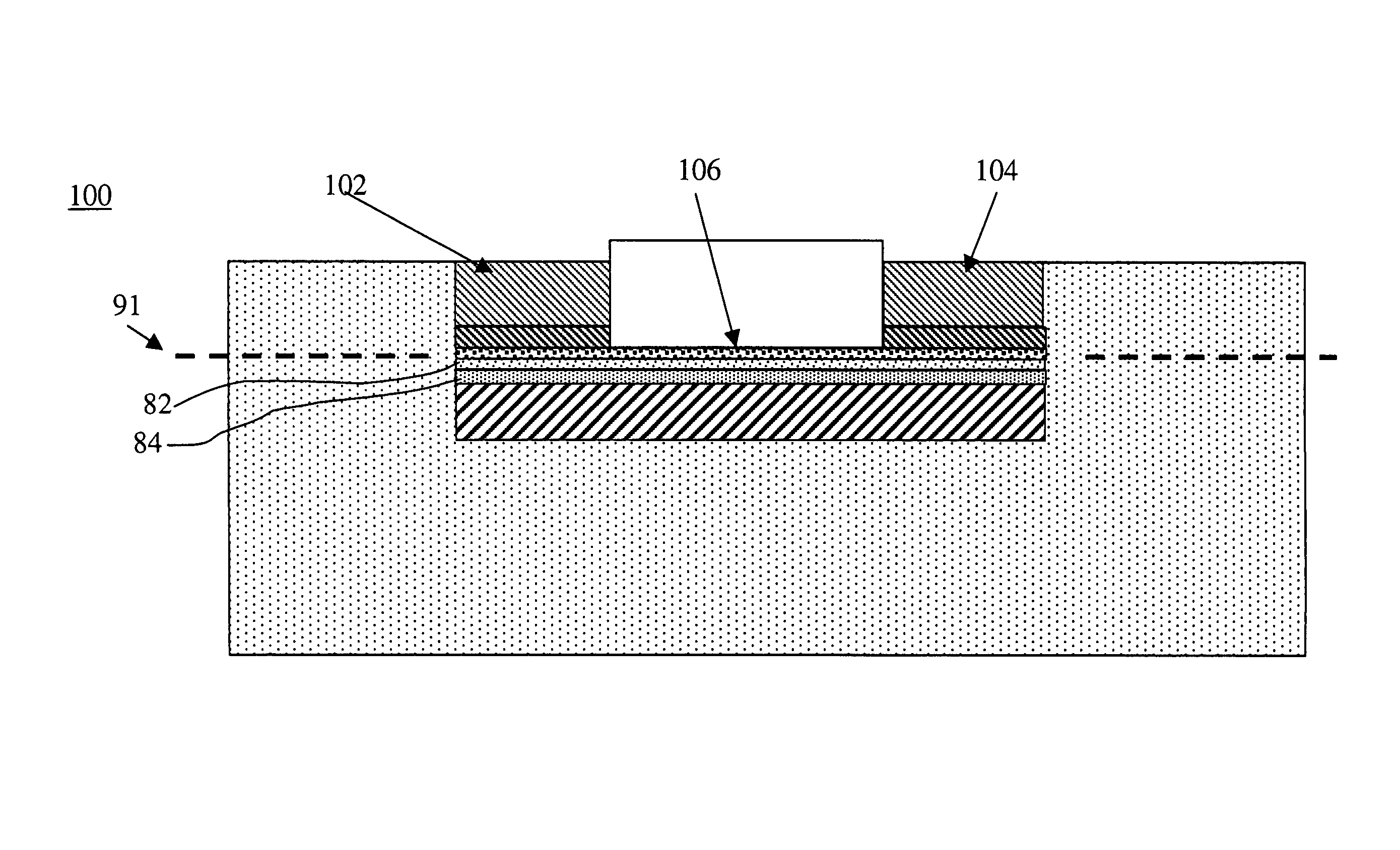
[0054]The current device layout is similar to that of the 3-terminal NRAM device. The FET properties represent a new operational mode for th...


PUM


Abstract

Field effect devices having channels of nanofabric and methods of making same. A nanotube field effect transistor is made to have a substrate, and a drain region and a source region in spaced relation relative to each other. A channel region is formed from a fabric of nanotubes, in which the nanotubes of the channel region are substantially all of the same semiconducting type of nanotubes. At least one gate is formed in proximity to the channel region so that the gate may be used to modulate the conductivity of the channel region so that a conductive path may be formed between the drain and source region. Forming a channel region includes forming a fabric of nanotubes in which the fabric has both semiconducting and metallic nanotubes and the fabric is processed to remove substantially all of the metallic nanotubes.

Description

CROSS-REFERENCE OF RELATED CASES[0001]This application claims the benefit under 35 U.S.C. §119(e) of U.S. Provisional Patent Application No. 60 / 644,427, filed on Jan. 14, 2005, entitled Field Effect Device Having a Channel of Carbon Nanofabric and Method of Making Same, and U.S. Provisional Patent Application No. 60 / 644,641, filed on Jan. 18, 2005, entitled Hybrid Carbon Nanotubes FET (CNFET)-FET Static RAM (SRAM), the contents of which are hereby incorporated by reference in their entireties.[0002]This application is related to U.S. patent application Ser. No. 11 / 332,080, filed on an even date herewith, entitled Hybrid Carbon Nanotubes FET (CNFET)-FET Static RAM (SRAM), the contents of which is hereby incorporated by reference in its entirety.BACKGROUND[0003]1. Technical Field[0004]This invention relates in to a field effect device having an channel of carbon nanofabric and a method of making the same.[0005]2. Discussion of Related Art[0006]Scaling of CMOS FETs is increasingly diff...

Claims


Application Information

Patent Timeline
Patent Type & Authority Patents(United States)
IPC IPC(8): H01L21/335H01L29/76H01L21/336
CPCB82Y10/00H01L21/823807H10K85/221H10K85/615H10K10/46H10K10/464
Inventor BERTIN, CLAUDE L.MEINHOLD, MITCHELLKONSEK, STEVEN L.RUECKES, THOMASGUO, FRANK
Owner NANTERO
Why Eureka
Try Eureka