

Semiconductor device
a semiconductor device and semiconductor technology, applied in the direction of semiconductor devices, basic electric elements, electrical equipment, etc., can solve the problems of reducing the speed of miniaturization of semiconductor devices, affecting the improvement of operating frequency, so as to increase the drain current
- Summary
- Abstract
- Description
- Claims
- Application Information
AI Technical Summary
Benefits of technology
Problems solved by technology
Method used
Image

Examples
first embodiment
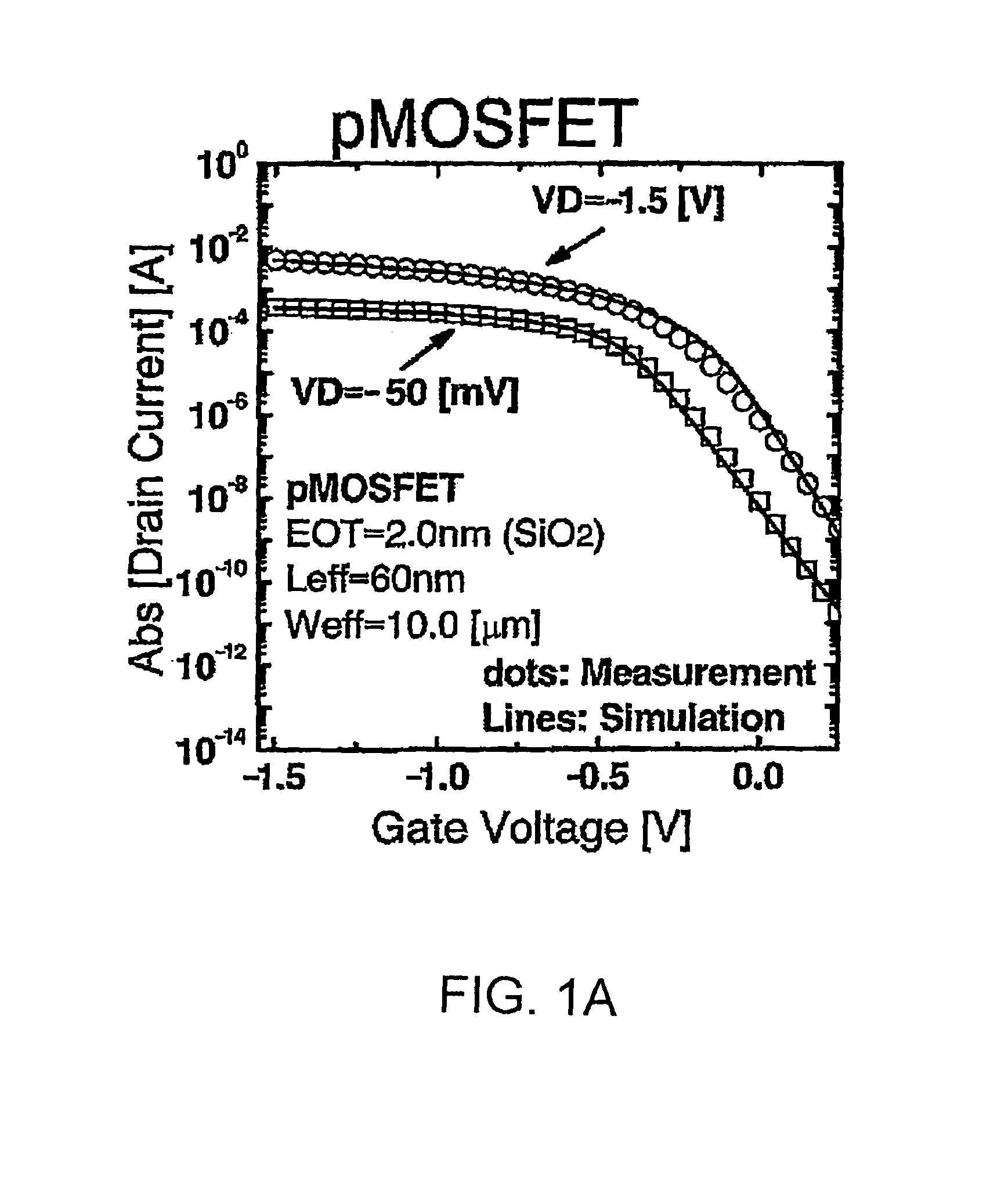
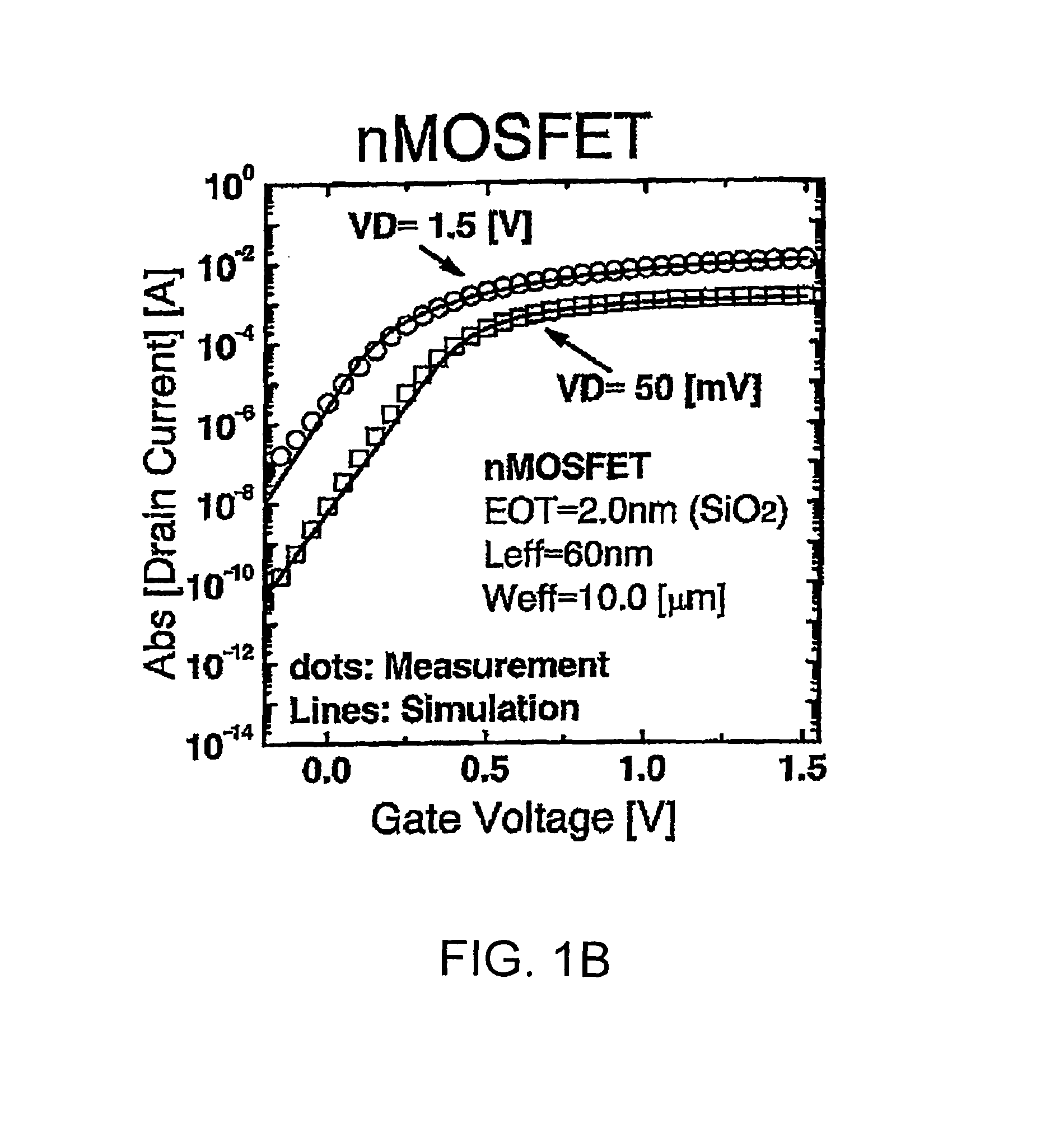
[0163]Referring to FIG. 14, there is illustrated a specific structural example of a MOSFET according to a first embodiment of this invention. The MOSFET illustrated in FIG. 14 is an nMOSFET having a buried insulating layer (BOX) 52 on a p-type silicon substrate or a metal substrate 51 and an SOI layer 53 formed on the BOX 52. Herein, the BOX 52 has a thickness of 10.0 nm and is formed of SiO2, while, the SOI layer 53 is in the form of an n+ silicon layer having a thickness of 20.0 nm. The SOI layer 53 is formed with a channel region 530 having an impurity concentration of 3×1018 cm−3 and a source region 531 and a drain region 532 formed on both sides of the channel region 530 and each having a higher concentration than that of the channel region. The channel region 530 has a channel length L of 0.50 μm. Further, a gate insulating film 54 formed of silicon nitride and having a SiO2 equivalent thickness (EOT) of 1.0 nm is formed on the surface of the channel region 530 and a gate elec...
second embodiment
[0165]Next, referring to FIGS. 15A to 15C, a semiconductor device forming a CMOS circuit including an nMOSFET and a pMOSFET will be described as a second embodiment of this invention.
[0166]FIG. 15A is a schematic perspective view of the semiconductor device according to the second embodiment of this invention. FIG. 15B shows a sectional view taken along line A-A′ in FIG. 15A and FIG. 15C shows a sectional view taken along line B-B′ in FIG. 15A.
[0167]The second embodiment is an SOI-type three-dimensional structure CMOS device designed to balance the current driving capabilities with the same size. In this CMOS device, a pMOSFET (p-channel transistor) is fabricated only on the (551) plane where the hole mobility is large and the surface flattening is facilitated, while, an nMOSFET is fabricated on the (551) plane, where the electron mobility is slightly inferior, with its gate formed also at side walls having a plane offset by 4° from the (100) plane where the electron mobility is lar...
PUM
 Abstract
Description
Claims
Application Information