4h-sic metal-semiconductor field-effect transistor with sloped gate and manufacturing method

A field-effect transistor and metal-semiconductor technology, which is applied in the field of 4H-SiC metal-semiconductor field-effect transistors and fabrication, can solve the problems of limited increase in device breakdown voltage, reduced device breakdown voltage, etc. Reduced channel resistance and small depletion area

Active Publication Date: 2017-10-13
XIDIAN UNIV
View PDF5 Cites 1 Cited by
  • Summary
  • Abstract
  • Description
  • Claims
  • Application Information

AI Technical Summary

Problems solved by technology

However, the improvement of the traditional 4H-SiCMESFET geometry is limited to the improvement of the breakdown voltage of the device. This is because the improvement of the breakdown voltage of the 4H-SiC MESEFT is limited by the saturation leakage current and the breakdown voltage under the condition of ensuring a large device current. Limitation of breakdown voltage equalization: Large saturation current density requires thicker channel and higher doping concentration, however, the increase of doping concentration and thickness will reduce the breakdown voltage of the device

Method used


Image

  • 4h-sic metal-semiconductor field-effect transistor with sloped gate and manufacturing method
  • 4h-sic metal-semiconductor field-effect transistor with sloped gate and manufacturing method

Examples


Embodiment 1

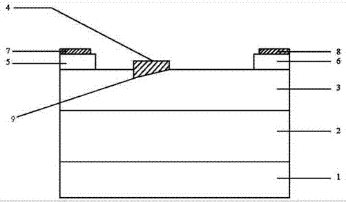
[0031] A 4H-SiC metal-semiconductor field-effect transistor with a 0.07 μm deep and 0.7 μm long sloped gate was fabricated.

[0032] The manufacturing steps of this embodiment are as follows:

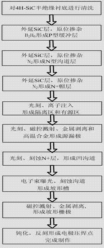
[0033] Step 1: cleaning the 4H-SiC semi-insulating substrate 1 to remove surface pollutants.

[0034] (1.1) Carefully wash the substrate twice with a cotton ball dipped in methanol to remove SiC particles of various sizes on the surface;

[0035] (1.2) Place the substrate in H 2 SO 4 :HNO 3 = Ultrasound for 5 minutes in 1:1;

[0036] (1.3) Put the substrate in 1# cleaning solution (NaOH:H 2 o 2 :H 2 O=1:2:5), boiled for 5 minutes, rinsed with deionized water for 5 minutes, and then put into 2# cleaning solution (HCl:H 2 o 2 :H 2 O=1:2:7) and boiled for 5 minutes. Finally rinsed with deionized water and rinsed with N 2 Blow dry and set aside.

[0037] Step 2: epitaxially grow a SiC layer on the surface of the 4H-SiC semi-insulating substrate 1, and diborane B 2 h 6 In-situ...

Embodiment 2

[0071] A 4H-SiC metal-semiconductor field-effect transistor with a sloped gate 0.06 μm deep and 0.7 μm long was fabricated.

[0072] In the manufacturing steps of this embodiment:

[0073] Step 8: Form a slope-shaped groove 9 on the concave channel between the source electrode 7 and the drain electrode 8 .

[0074] 1) Under the conditions of glue coating speed: 3000R / min, glue thickness > 2μm, use positive photoresist to carry out photolithography on the concave groove, make a photolithography plate according to the position of the slope grid, and expose it with electron beam;

[0075] 2) In special developer solution ((CH 3 ) 4 NOH:H 2 In O=1:4), the channel is developed, and the pattern on the photolithography plate is transferred to the concave channel between the source region and the drain region to form a gate pattern window, and then the reactive ion etching process is used to etch the concave groove At the same time, a groove with a length of 0.7 μm, a distance of ...

Embodiment 3

[0082] Embodiment 3: Fabricate a 4H-SiC metal-semiconductor field-effect transistor with a 0.08 μm deep and 0.7 μm long slope gate.

[0083] In the manufacturing steps of this embodiment:

[0084] Step 8: Form a slope-shaped groove 9 on the concave channel between the source electrode 7 and the drain electrode 8 .

[0085] 1) Under the conditions of coating speed: 3000R / min and glue thickness > 2μm, use positive photoresist to perform photolithography on the concave groove, make a photolithography plate according to the position of the slope grid, and expose it with electron beams;

[0086] 2) In special developer solution ((CH 3 ) 4 NOH:H 2 In O=1:4), the channel is developed, and the pattern on the photolithography plate is transferred to the concave channel between the source region and the drain region to form a gate pattern window, and then the reactive ion etching process is used to etch the concave groove At the same time, a groove with a length of 0.7 μm, a distanc...


PUM


Abstract

The invention discloses a 4H-SiC metal semiconductor field effect transistor with a slope-shaped grid. The 4H-SiC metal semiconductor field effect transistor comprises a 4H-SiC semi-insulating substrate, a P-type buffer layer and an N-type channel layer from bottom to top, a source electrode cap layer and a drain electrode cap layer are arranged on the surface of the N-type channel layer, a source electrode and a drain electrode are arranged on the surface of the source electrode cap layer and the surface of the drain electrode cap layer respectively, a slope-shaped groove inclined towards one side of the source electrode cap layer is formed in the upper end face of the N-type channel layer, the slope-shaped grid is arranged is arranged in the slope-shaped groove, the lower end face of the slope-shaped grid is matched with the slope-shaped groove, the upper end face of the slope-shaped grid is parallel to the upper end face of the N-type channel layer, and the distance between the slope-shaped grid and the source electrode cap layer is smaller than that between the slope-shaped grid and the drain electrode cap layer. The field effect transistor has the advantages of being high in drain electrode output current and excellent in frequency property.

Description

technical field [0001] The invention relates to a field effect transistor, in particular to a 4H-SiC metal semiconductor field effect transistor with a slope gate and a manufacturing method. Background technique [0002] Due to its outstanding material and electrical properties, such as large band gap, high saturation electron migration velocity, high breakdown electric field, high thermal conductivity, etc., SiC is used in high frequency and high power device applications, especially at high temperature, It has great potential in the application of high-frequency and high-power devices in harsh environments such as high voltage, aerospace, and satellite. SiC plays a major role in the application of microwave power devices, especially metal-semiconductor field-effect transistors (MESFETs). [0003] The structure of the traditional 4H-SiC MESFET is from bottom to top: 4H-SiC semi-insulating substrate, P-type buffer layer, N-type channel layer and N+ cap layer, after etching ...

Claims


Application Information

Patent Timeline
Patent Type & Authority Patents(China)
IPC IPC(8): H01L29/78H01L21/336H01L29/10
CPCH01L29/1037H01L29/24H01L29/66477H01L29/78
Inventor 贾护军刑鼎张航
Owner XIDIAN UNIV
Why Eureka
Try Eureka