Field effect transistor with gamma gate and recessed buffer layer and its preparation method

A technology of field effect transistors and buffer layers, which is applied in semiconductor devices, electrical components, circuits, etc., can solve the problems of no substantial improvement of saturation leakage current, decrease of effective carrier mobility, and reduction of drain current, etc., to achieve The effects of increased breakdown voltage, increased saturation leakage current, and reduced gate-to-drain capacitance

Active Publication Date: 2018-06-26
XIDIAN UNIV
View PDF3 Cites 0 Cited by
  • Summary
  • Abstract
  • Description
  • Claims
  • Application Information

AI Technical Summary

Problems solved by technology

[0004] Although the breakdown voltage of the 4H-SiC MESFET with the double-recessed structure is increased due to the fact that half the length of the source side of the gate is recessed into the N-type channel layer, the saturation leakage current has not been substantially improved.
And in practice, the process of reactive ion etching (RIE) will form lattice damage on the surface of the drift region of the device, resulting in a decrease in the effective mobility of carriers in the N-type channel layer, thereby reducing the drain current. In terms of current output characteristics manifested as a degradation of the saturation current

Method used


Image

  • Field effect transistor with gamma gate and recessed buffer layer and its preparation method

Examples


Embodiment 1

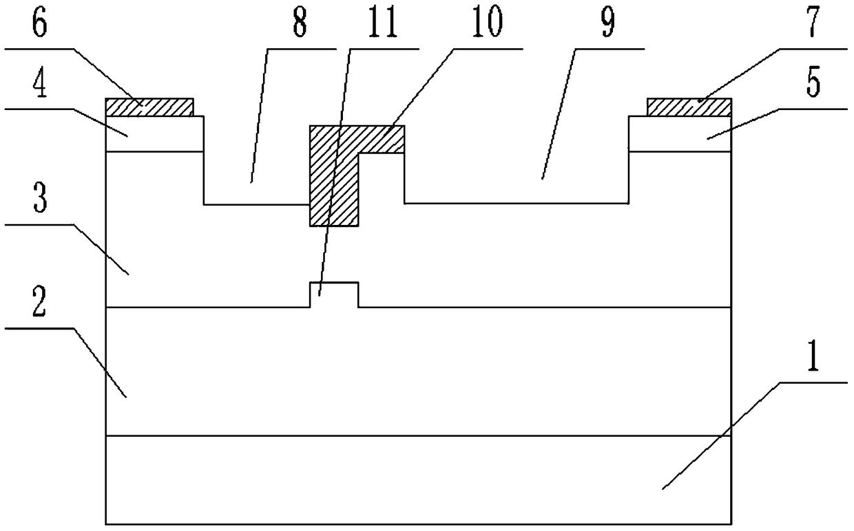
[0039] A field effect transistor with a Γ gate and a recessed buffer layer having a groove 11 with a height and a length of 0.05 μm and 0.35 μm was prepared. Follow the steps below:

[0040]Step 1) cleaning the 4H-SiC semi-insulating substrate 1 to remove dirt on the surface of the substrate;

[0041] a. Carefully clean the substrate two or three times with a cotton ball dipped in methanol to remove SiC particles of various sizes on the surface;

[0042] b. Place 4H-SiC semi-insulating substrate 1 in H 2 SO 4 :HNO 3 = Ultrasound for 5 minutes in 1:1;

[0043] c. Put the 4H-SiC semi-insulating substrate 1 in 1# cleaning solution (NaOH:H 2 o 2 :H 2 O=1:2:5) and boiled for 5 minutes, then rinsed with deionized water for 5 minutes and then put into 2# cleaning solution (HCl:H 2 o 2 :H 2 O=1:2:7) and boiled for 5 minutes, finally rinsed with deionized water and blow-dried with N2 for later use.

[0044] Step 2) epitaxially grow a 0.5 μm thick SiC layer on the 4H-SiC semi...

Embodiment 2

[0081] Field effect transistors with a Γ gate and a recessed buffer layer were fabricated with groove heights and lengths of 0.05 μm and 0.3 μm. The difference between this embodiment and Embodiment 1 lies in step 8)

[0082] a. Positive photoresist is used, the coating speed is 3000R / min, and the thickness of the glue is >2μm to ensure that it can play a good blocking role in the subsequent isolation injection;

[0083] b. After the gluing is completed, pre-bake in an oven at 90°C for 90 seconds, use a sunken buffer layer photolithography plate for about 35 seconds of ultraviolet exposure, and then develop in a special developer for 60 seconds. The formula of the special developer: tetramethylammonium hydroxide: Water = 1:3, then post-bake in an oven at 100°C for 3 minutes;

[0084] c. Carry out boron ion implantation, the implantation condition is 300keV / 2×10 12 cm -2 , the temperature is 400°C. After the injection is completed, use acetone and ultrasonic to remove the g...

Embodiment 3

[0087] A field effect transistor with a Γ gate and a recessed buffer layer with a groove height and length of 0.05 μm and 0.4 μm was prepared. The difference between this embodiment and Embodiment 1 lies in step 8).

[0088] a. Positive photoresist is used, the coating speed is 3000R / min, and the thickness of the glue is >2μm to ensure that it can play a good blocking role in the subsequent isolation injection;

[0089] b. After the gluing is completed, pre-bake in an oven at 90°C for 90 seconds, use a sunken buffer layer photolithography plate for about 35 seconds of ultraviolet exposure, and then develop in a special developer for 60 seconds. The formula of the special developer: tetramethylammonium hydroxide: Water = 1:3, then post-bake in an oven at 100°C for 3 minutes;

[0090] c. Carry out boron ion implantation, the implantation condition is 300keV / 2×10 12 cm -2 , the temperature is 400°C. After the injection is completed, use acetone and ultrasonic to remove the gl...


PUM


Abstract

The invention belongs to the technical field of field effect transistors and provides a field effect transistor equipped with a gamma-gate and a recessed buffer layer and a preparation method thereof, wherein the field effect transistor has a wide channel and a deep recess and is increased in output current and breakdown voltage and improved in frequency characteristic. An employed technical scheme is that a 4F-SiC semi-insulated substrate, a P-type buffer layer, an N-type channel layer are arranged from top to bottom; a source electrode cap layer and a drain electrode cap layer are arranged on both sides of the N-type channel layer respectively; the surface of the source electrode cap layer and the surface of the drain electrode cap layer are provided with a source electrode and a drain electrode respectively; a stepped gate electrode is disposed on a side, close to the source electrode cap layer, of the middle of the N-type channel layer; a left channel and a right channel are formed between both sides of the N-type channel layer and the gate electrode respectively; the low gate surface of the gate electrode is flush with the surface of the N-type channel layer; and a groove is disposed on the P-type buffer layer right under the low gate surface of the gate electrode.

Description

technical field [0001] The invention belongs to the technical field of field effect transistors, in particular to a field effect transistor with a Γ gate and a recessed buffer layer and a preparation method thereof. Background technique [0002] SiC materials have outstanding material and electrical properties such as wide band gap, high breakdown electric field, high saturated electron migration velocity, and high thermal conductivity, making them suitable for high-frequency and high-power device applications, especially high temperature, high voltage, aerospace, satellite, etc. It has great potential in high-frequency high-power device applications in harsh environments. In SiC allomorphs, the electron mobility of 4H-SiC with hexagonal close-packed wurtzite structure is nearly three times that of 6H-SiC, so 4H-SiC materials are used in high-frequency and high-power devices, especially in metal-semiconductor fields. Effect transistor (MESFET) occupies a major position in t...

Claims


Application Information

Patent Timeline
Patent Type & Authority Patents(China)
IPC IPC(8): H01L29/78H01L29/10H01L29/66H01L29/423
CPCH01L29/1037H01L29/4232H01L29/66477H01L29/78
Inventor 贾护军张航邢鼎杨银堂
Owner XIDIAN UNIV
Why Eureka
Try Eureka