4h-sic metal-semiconductor field-effect transistor with stepped buffer layer structure

A field-effect transistor and metal-semiconductor technology, which is applied in the field of 4H-SiC metal-semiconductor field-effect transistors, can solve problems such as no increase in saturation leakage current, lattice damage, and reduced drain current.

Active Publication Date: 2017-06-30
XIDIAN UNIV
View PDF4 Cites 0 Cited by
  • Summary
  • Abstract
  • Description
  • Claims
  • Application Information

AI Technical Summary

Problems solved by technology

[0004] Compared with the double recessed structure, although the breakdown voltage of the above-mentioned recessed source / drain drift region 4H-SiC MESFET is increased due to the reduction of the thickness of the drift region between the gate and drain, the saturation leakage current is not improved
And in practice, the process of reactive ion etching (RIE) will form lattice damage on the surface of the drift region of the device, resulting in a decrease in the effective mobility of carriers in the N-type channel layer, thereby reducing the drain current. In terms of current output characteristics manifested as a degradation of the saturation current

Method used


Image

  • 4h-sic metal-semiconductor field-effect transistor with stepped buffer layer structure
  • 4h-sic metal-semiconductor field-effect transistor with stepped buffer layer structure

Examples


Embodiment 1

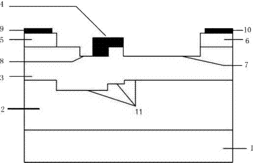
[0031] Example 1: Fabricate a 4H-SiC metal-semiconductor field-effect transistor with a thickness of 0.53 μm and a stepped P-type buffer layer with two steps 11 of 0.03 μm and 0.05 μm.

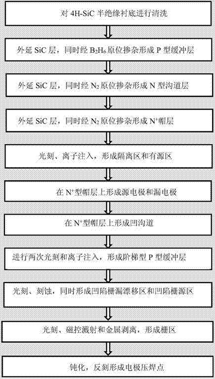
[0032] The manufacturing steps of this embodiment are as follows:

[0033] Step 1: cleaning the 4H-SiC semi-insulating substrate 1 to remove surface pollutants.

[0034] (1.1) Carefully wash the substrate twice with a cotton ball dipped in methanol to remove SiC particles of various sizes on the surface;

[0035] (1.2) Place 4H-SiC semi-insulating substrate 1 in H 2 SO 4 :HNO 3 = Ultrasound for 5 minutes in 1:1;

[0036] (1.3) Put 4H-SiC semi-insulating substrate 1 in 1# cleaning solution (NaOH:H 2 o 2 :H 2 O=1:2:5), boiled for 5 minutes, rinsed with deionized water for 5 minutes, and then put into 2# cleaning solution (HCl:H 2 o 2 :H 2 O=1:2:7) and boiled for 5 minutes. Finally rinsed with deionized water and rinsed with N 2 Blow dry and set aside.

[0037] Step 2: Epitaxially gr...

Embodiment 2

[0077] Embodiment 2: Fabricate a 4H-SiC metal-semiconductor field-effect transistor with a thickness of 0.52 μm and a stepped P-type buffer layer with two steps of 0.03 μm and 0.03 μm. In the manufacturing steps of this embodiment:

[0078] Step 2: Epitaxially grow a SiC layer on the surface of the 4H-SiC semi-insulating substrate 1, while diborane B 2 h 6 In-situ doping forms the P-type buffer layer 2 .

[0079] Put the 4H-SiC semi-insulating substrate 1 into the growth chamber, and feed silane with a flow rate of 20ml / min, propane with a flow rate of 10ml / min and high-purity hydrogen with a flow rate of 80l / min into the growth chamber, and simultaneously feed 2ml / min of B 2 h 6 (H 2 diluted to 5%), the growth temperature was 1550°C, and the pressure was 10 5 Pa, last for 6min, complete doping concentration and thickness are 1.4×10 15 cm -3 and a P-type buffer layer 2 of 0.52 μm.

[0080] Step 3: epitaxially grow the SiC layer on the P-type buffer layer 2, and at the ...

Embodiment 3

[0089] Embodiment 3: Fabricate a 4H-SiC metal-semiconductor field-effect transistor with a thickness of 0.55 μm and a stepped P-type buffer layer with two steps of 0.05 and 0.05 μm. In the manufacturing steps of this embodiment:

[0090] Step 2: Epitaxial growth of SiC layer on the surface of 4H-SiC semi-insulating substrate, while diborane B 2 h 6 In-situ doping forms a P-type buffer layer.

[0091] Put the 4H-SiC semi-insulating substrate 1 into the growth chamber, and feed silane with a flow rate of 20ml / min, propane with a flow rate of 10ml / min and high-purity hydrogen with a flow rate of 80l / min into the growth chamber, and simultaneously feed 2ml / min of B 2 h 6 (H 2 diluted to 5%), the growth temperature was 1550°C, and the pressure was 10 5 Pa, last for 6min, complete doping concentration and thickness are 1.4×10 15 cm -3 and a P-type buffer layer 2 of 0.55 μm.

[0092] Step 3: epitaxially grow the SiC layer on the P-type buffer layer 2, and at the same time 2 ...


PUM


Abstract

The invention discloses a 4H-SiC metal semiconductor field effect transistor with a step buffer layer structure. The 4H-SiC metal semiconductor field effect transistor comprises a 4H-SiC semi-insulating substrate, a P-type buffer layer and an N-type channel layer from the bottom to the top. The two sides of the N-type channel layer are respectively provided with a source electrode cap layer and a drain electrode cap layer. The surface of the source electrode cap layer and the drain electrode cap layer is respectively provided with a source electrode and a drain electrode. A gate electrode is formed on one side which is arranged above the N-type channel layer and close to the source electrode cap layer. A concave gate source drift region is formed between the gate electrode and the source electrode cap layer. A concave gate drain drift region is formed between the gate electrode and the drain electrode cap layer. The position, which is arranged on the upper end surface of the P-type buffer layer and close to the source electrode cap layer, is provided with a groove. One side, which is arranged in the groove and close to the drain electrode cap layer, is provided with two steps. The 4H-SiC metal semiconductor field effect transistor with the step buffer layer structure has advantages of being stable in breakdown voltage and high in output drain electrode current.

Description

technical field [0001] The invention relates to the technical field of field effect transistors, in particular to a 4H-SiC metal semiconductor field effect transistor with a ladder buffer layer structure. Background technique [0002] SiC materials have outstanding material and electrical properties such as wide band gap, high breakdown electric field, high saturated electron migration velocity, and high thermal conductivity, making them suitable for high-frequency and high-power device applications, especially high temperature, high voltage, aerospace, satellite, etc. It has great potential in high-frequency high-power device applications in harsh environments. In SiC allomorphs, the electron mobility of 4H-SiC with hexagonal close-packed wurtzite structure is nearly three times that of 6H-SiC, so 4H-SiC materials are used in high-frequency and high-power devices, especially in metal-semiconductor fields. Effect transistor (MESFET) occupies a major position in the applicat...

Claims


Application Information

Patent Timeline
Patent Type & Authority Patents(China)
IPC IPC(8): H01L29/78H01L29/06H01L21/336
CPCH01L29/0611H01L29/66068H01L29/812
Inventor 贾护军张航刑鼎
Owner XIDIAN UNIV
Why Eureka
Try Eureka