Method for making light emitting diode

Active Publication Date: 2013-02-19
TSINGHUA UNIV +1
View PDF8 Cites 4 Cited by
  • Summary
  • Abstract
  • Description
  • Claims
  • Application Information

AI Technical Summary

Benefits of technology

The patent describes a type of structure that protrudes from a substrate surface. These structures can be made from the same or different materials as the substrate. They can be attached to or integrated with the substrate to form a single structure. The "technical effect" of this patent is the creation of a new type of structure that can be used in various applications, such as electronics or sensors, that improves performance and efficiency.

Problems solved by technology

However, extraction efficiency of LEDs is low because typical semiconductor materials have a higher refraction index than that of air.

Method used


Image

  • Method for making light emitting diode
  • Method for making light emitting diode
  • Method for making light emitting diode

Examples


Embodiment Construction

[0022]The disclosure is illustrated by way of example and not by way of limitation in the figures of the accompanying drawings in which like references indicate similar elements. It should be noted that references to “an” or “one” embodiment in this disclosure are not necessarily to the same embodiment, and such references mean at least one.

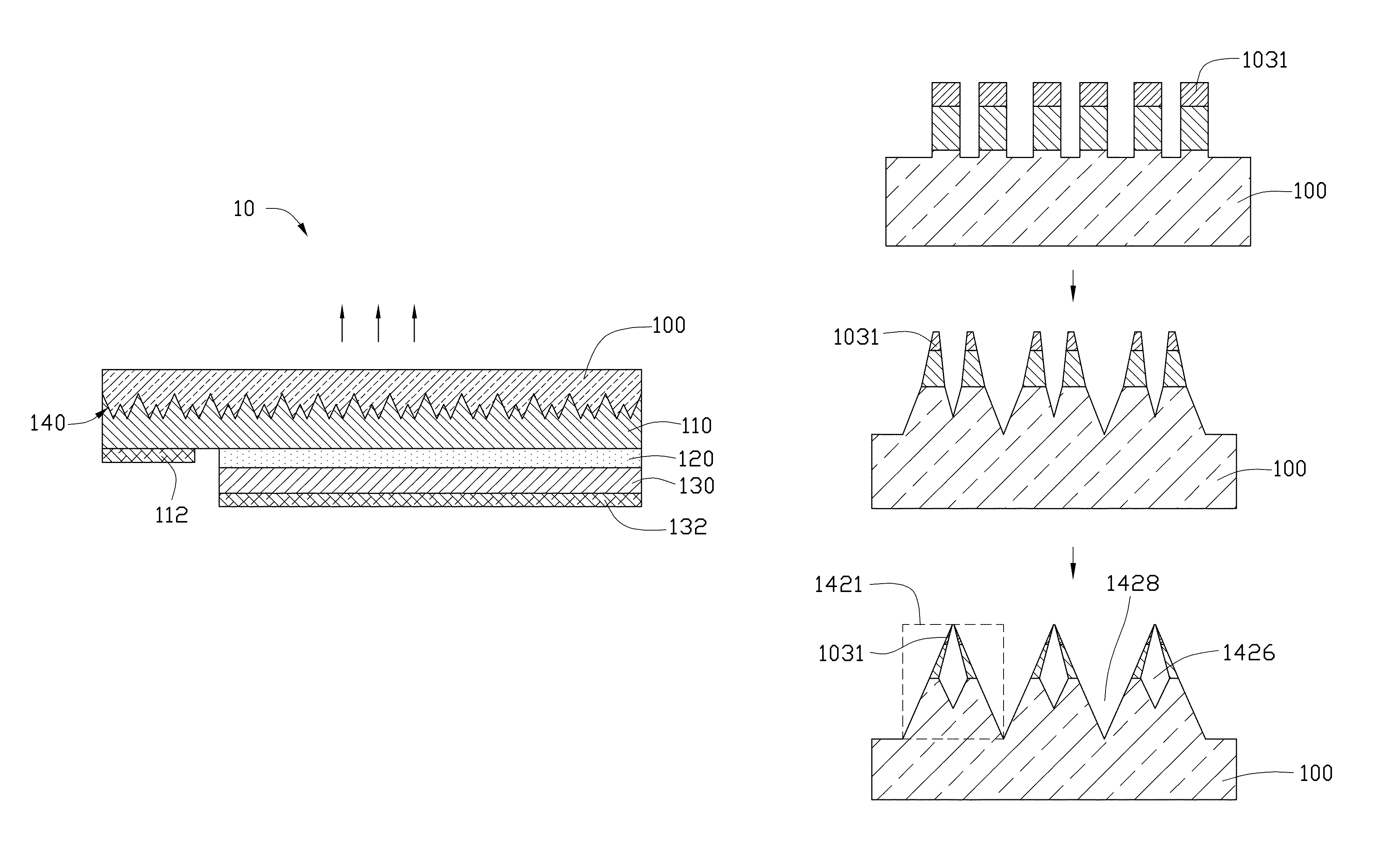
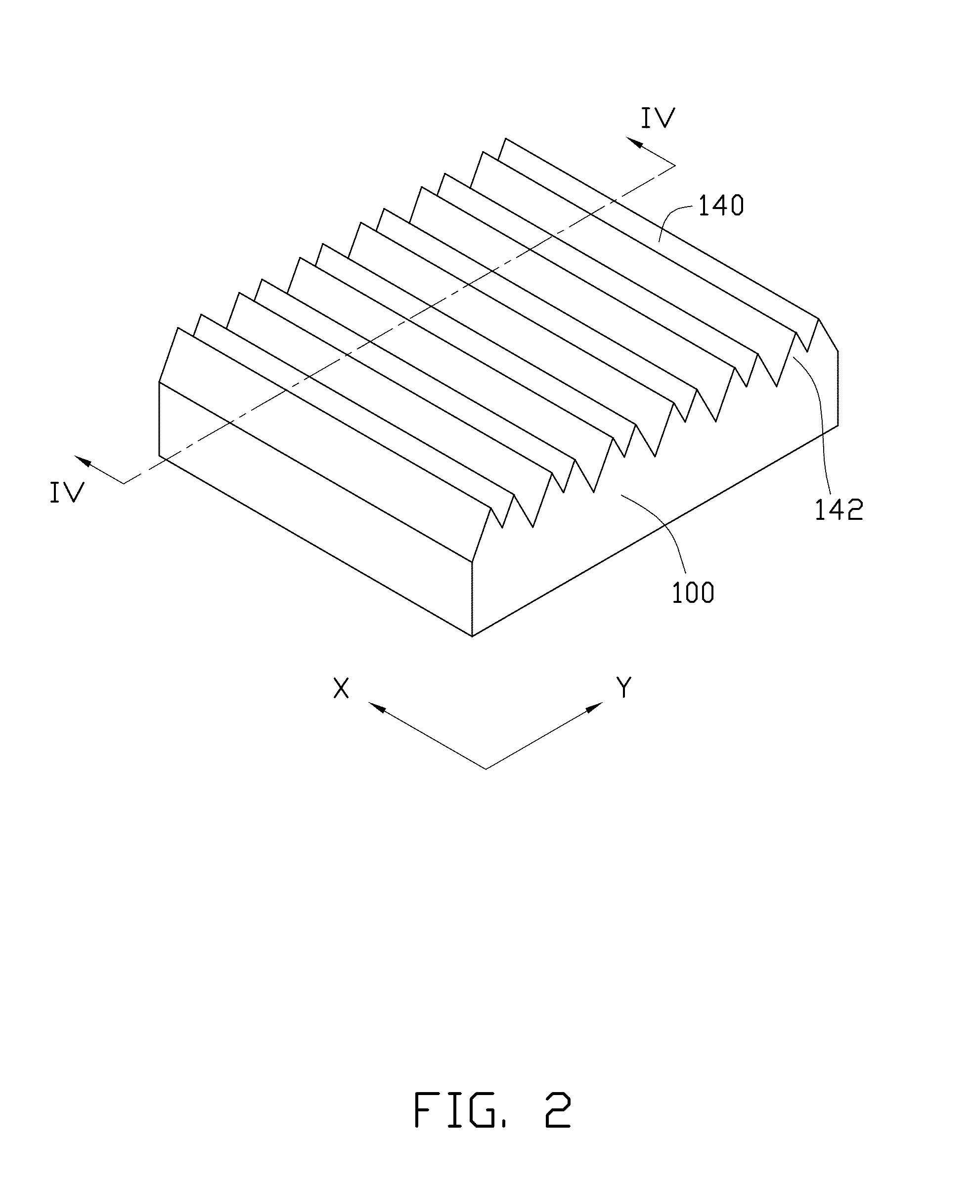
[0023]Referring to FIG. 1, an LED 10 includes a substrate 100, a first semiconductor layer 110, an active layer 120 and a second semiconductor layer 130, a first electrode 112, a second electrode 132 and a three-dimensional nano-structure array 140. The substrate 100 includes a first surface and the second surface opposite to the first surface. The first semiconductor layer 110, the active layer 120 and the second semiconductor layer 130 are stacked on the first surface of the substrate 100 in that order, and the first semiconductor layer 110 is contacted with the substrate 100. The second surface is used as the light emitting surface of the LED ...


PUM


Abstract

A method for making light emitting diode is provided. The method includes following steps. A substrate is provided. A patterned mask layer is located on a surface of the substrate, and the patterned mask layer includes a number of bar-shaped protruding structures aligned side by side, a slot is defined between each two adjacent protruding structures to expose a portion of the substrate. The exposed substrate is etched, and each two adjacent protruding structures begin to slant face to face until closed to form a protruding pair. A number of three-dimensional nano-structures are formed by removing the patterned mask layer. A first semiconductor layer, an active layer and a second semiconductor layers are grown on the number of three-dimensional nano-structures in that order. A first electrode is electrically connected with the first semiconductor layer. A second electrode is electrically connected with the second semiconductor layer.

Description

CROSS-REFERENCE TO RELATED APPLICATIONS[0001]This application claims all benefits accruing under 35 U.S.C. §119 from China Patent Application No. 201114293096.1, filed on Oct. 7, 2011 in the China Intellectual Property Office, disclosure of which is incorporated herein by reference. This application is related to applications entitled, “LIGHT EMITTING DIODE”, filed Dec. 29, 2011, U.S. application Ser. No. 13 / 340,627; “METHOD FOR MAKING LIGHT EMITTING DIODE”, filed Dec. 29, 2011, U.S. application Ser. No. 13 / 340,658; “LIGHT EMITTING DIODE”, filed Dec. 29, 2011, U.S. application Ser. No. 13 / 340,661; “METHOD FOR MAKING LIGHT EMITTING DIODE”, filed Dec. 29, 2011, U.S. application Ser. No. 13 / 340,662, “LIGHT EMITTING DIODE”, filed Dec. 29, 2011, U.S. application Ser. No. 13 / 340,643.BACKGROUND[0002]1. Technical Field[0003]The present disclosure relates to a light emitting diode (LED) and the method for making the same.[0004]2. Description of the Related Art[0005]LEDs are semiconductors th...

Claims


Application Information

Patent Timeline
IPC IPC(8): H01L21/00
CPCH01L33/44H01L33/22H01L33/007
Inventor ZHU, ZHEN-DONGLI, QUN-QINGFAN, SHOU-SHAN
Owner TSINGHUA UNIV
Why Eureka
Try Eureka