Output enable signal generation circuit of semiconductor memory

a technology of output enable and signal generation circuit, which is applied in the direction of information storage, static storage, digital storage, etc., can solve the problems of reducing the margin of one side, oeb>00/b> may not be accurately generated or the activation thereof may not occur, and the clock signal and the operation voltage are limited

Active Publication Date: 2013-03-19
SK HYNIX INC
View PDF11 Cites 794 Cited by
  • Summary
  • Abstract
  • Description
  • Claims
  • Application Information

AI Technical Summary

Benefits of technology

[0025]An output enable signal generation circuit of a semiconductor memory which may secure both activation and deactivation margins of a period signal is described herein.

Problems solved by technology

Referring to FIG. 6, however, when the delay time of the second delay DLY2 is set to an excessively large value to secure a margin and the read signal RDR overlaps the low level period of a signal OEBPU (refer to FIG. 2), a rising edge of the period signal OE00 may not be accurately generated or the activation thereof may not occur.
Therefore, a trade-off problem occurs in which when a margin for any one of the activation time and deactivation time of the period signal is secured, a margin for the other is reduced.
As a result, the clock signal and the operation voltage are limited and degrade the characteristic of circuit operation.

Method used


Image

  • Output enable signal generation circuit of semiconductor memory
  • Output enable signal generation circuit of semiconductor memory
  • Output enable signal generation circuit of semiconductor memory

Examples


Embodiment Construction

[0039]Reference will now be made in detail to the exemplary embodiments consistent with the present disclosure, examples of which are illustrated in the accompanying drawings. Wherever possible, the same reference characters will be used throughout the drawings to refer to the same or like parts.

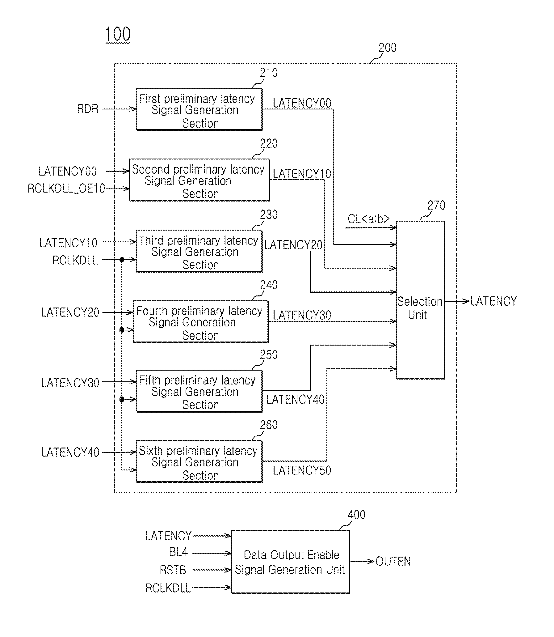
[0040]FIG. 7 is a block diagram of an output enable signal generation circuit of a semiconductor memory according to one embodiment. Referring to FIG. 7, an output enable signal generation circuit 100 of a semiconductor memory according to one embodiment includes a latency signal generation unit 200 and a data output enable signal generation unit 400.

[0041]The latency signal generation unit 200 is configured to generate a latency signal LATENCY which designates the activation timing of a data output enable signal OUTEN in response to a read signal RDR and a CAS latency signal CL.

[0042]The latency signal generation unit 200 includes a plurality of preliminary latency signal generation section...


PUM


Abstract

An output enable signal generation circuit of a semiconductor memory includes: a latency signal generation unit configured to generate a latency signal for designating activation timing of a data output enable signal in response to a read signal and a CAS latency signal; and a data output enable signal generation unit configured to control the activation timing and deactivation timing of the data output enable signal in response to the latency signal and a signal generated by shifting the latency signal based on a burst length (BL).

Description

CROSS-REFERENCES TO RELATED APPLICATION[0001]The present application claims priority under 35 U.S.C. §119(a) to Korean Application No. 10-2010-0063998, filed on Jul. 2, 2010, in the Korean Intellectual Property Office, which is incorporated herein by reference in its entirety as if set forth in full.BACKGROUND[0002]1. Technical Field[0003]The present invention relates to a semiconductor memory, and more particularly, to an output enable signal generation circuit of a semiconductor memory.[0004]2. Related Art[0005]A semiconductor memory uses an output enable signal to decide a window of data outputted based on a read operation. The output enable signal is generated within the semiconductor memory and used therein.[0006]FIG. 1 is a block diagram of an output enable signal generation circuit of a conventional semiconductor memory. Referring to FIG. 1, an output enable signal generation circuit 1 of a conventional semiconductor memory includes first to sixth period signal generation uni...

Claims


Application Information

Patent Timeline
Patent Type & Authority Patents(United States)
IPC IPC(8): G11C7/00
CPCG11C7/1051G11C7/1066G11C7/22G11C7/222G11C2207/2272
Inventor BYUN, HEE JIN
Owner SK HYNIX INC
Why Eureka
Try Eureka