Method of forming epi film in substrate trench

a substrate trench and epi film technology, applied in the direction of basic electric elements, electrical apparatus, semiconductor devices, etc., can solve the problems of n-channel strain limitation to problematic, current techniques to form these strained structures and channel-last transistors are not satisfactory in all respects, and no solution for ge p-channel strain has been found

Active Publication Date: 2013-04-09
TAIWAN SEMICON MFG CO LTD
View PDF44 Cites 178 Cited by
  • Summary
  • Abstract
  • Description
  • Claims
  • Application Information

AI Technical Summary

Problems solved by technology

However, current techniques to form these strained structures and channel-last transistors have not been satisfactory in all respects.
For example, Si N-channel strain is limited to problematic SiC films and no solution for Ge P-channel strain has been found.
It is even more challenging to realize epitaxy films for channel-last transistors with conventional epitaxial growth techniques.

Method used


Image

  • Method of forming epi film in substrate trench
  • Method of forming epi film in substrate trench
  • Method of forming epi film in substrate trench

Examples


Embodiment Construction

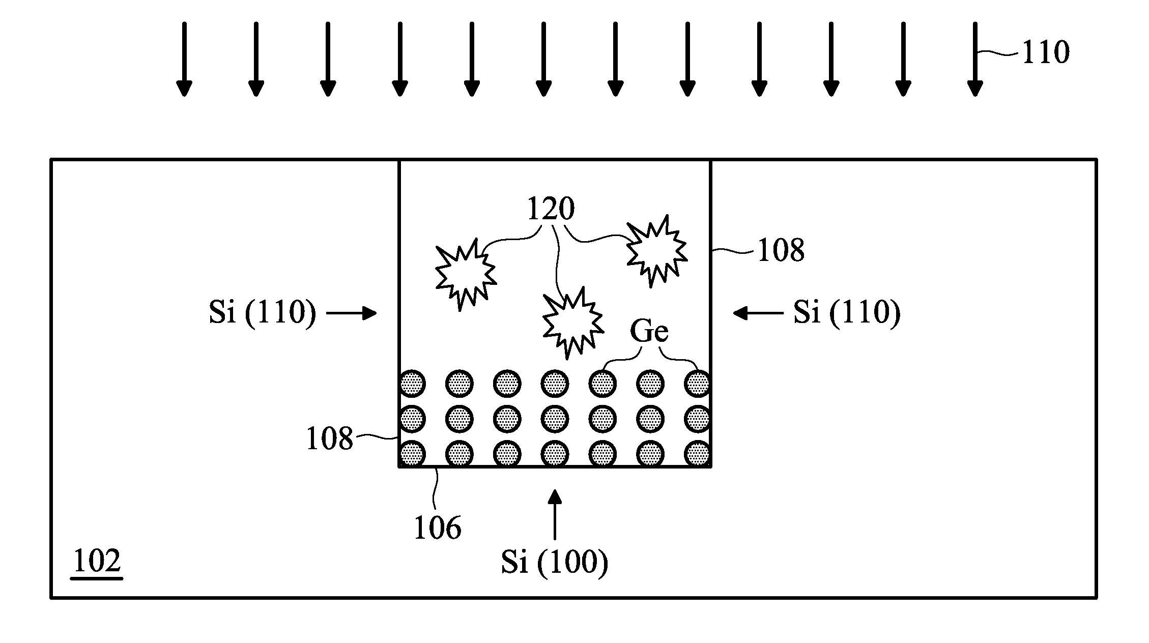
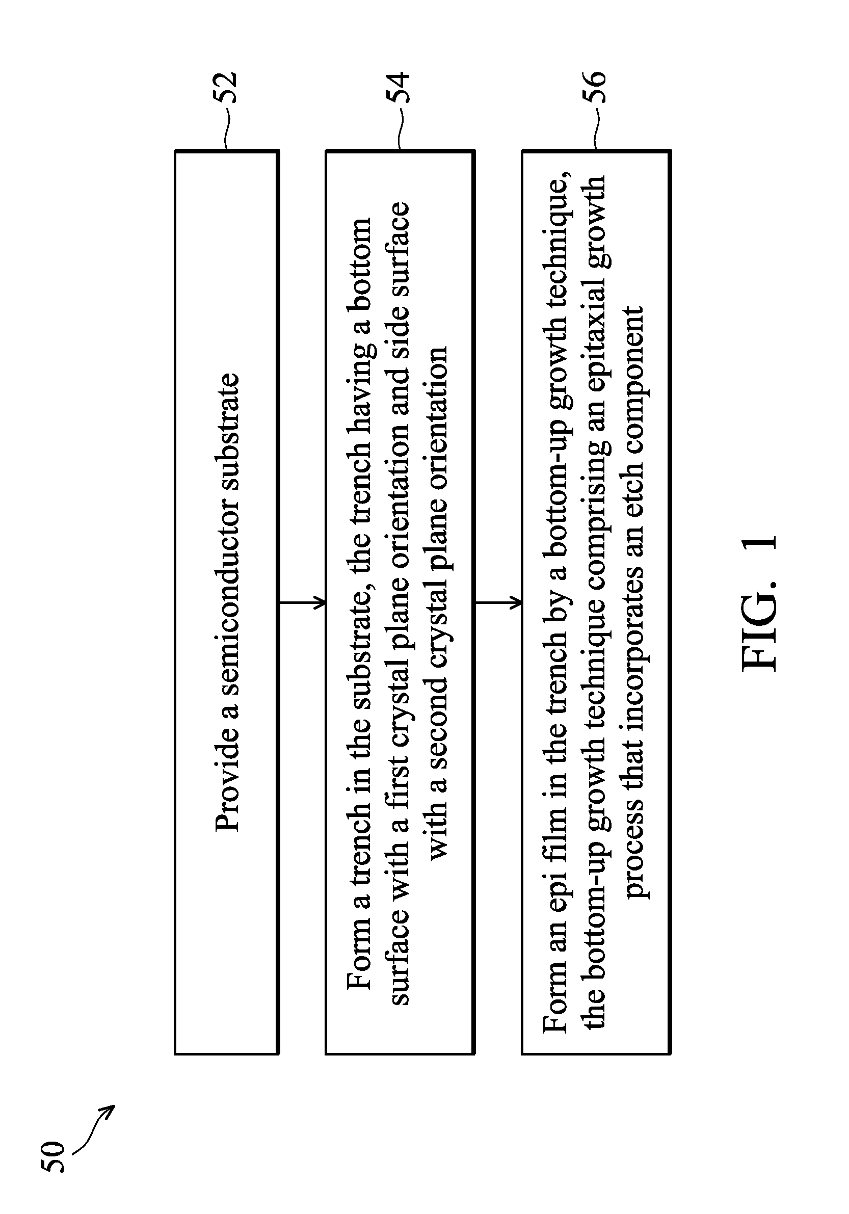
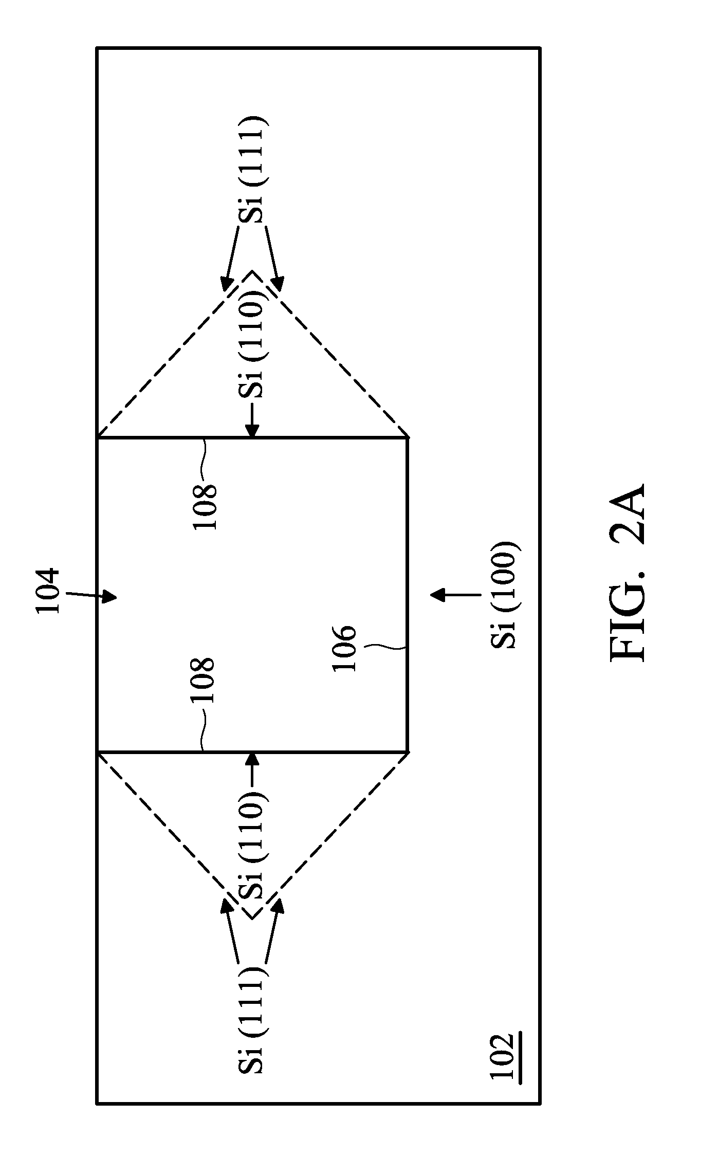
[0012]It is to be understood that the following disclosure provides many different embodiments, or examples, for implementing different features of various embodiments. Specific examples of components and arrangements are described below to simplify the present disclosure. These are, of course, merely examples and are not intended to be limiting. In addition, the present disclosure may repeat reference numerals and / or letters in the various examples. This repetition is for the purpose of simplicity and clarity and does not in itself dictate a relationship between the various embodiments and / or configurations discussed. Moreover, the formation of a first feature over or on a second feature in the description that follows may include embodiments in which the first and second features are formed in direct contact, and may also include embodiments in which additional features may be formed interposing the first and second features, such that the first and second features may not be in d...


PUM


Abstract

The present disclosure provides a method of fabricating a semiconductor device that includes providing a semiconductor substrate, forming a trench in the substrate, where a bottom surface of the trench has a first crystal plane orientation and a side surface of the trench has a second crystal plane orientation, and epitaxially (epi) growing a semiconductor material in the trench. The epi process utilizes an etch component. A first growth rate on the first crystal plane orientation is different from a second growth rate on the second crystal plane orientation.

Description

PRIORITY DATA[0001]This application claims priority to Provisional Application Ser. No. 61 / 256,431 filed on Oct. 30, 2009, the entire disclosure of which is incorporated herein by reference.BACKGROUND[0002]When a semiconductor device such as a metal-oxide-semiconductor field-effect transistors (MOSFETs) is scaled down through various technology nodes, high-k dielectric material and metal gate are adopted to form a gate stack. Strained structures utilizing epitaxy silicon germanium (SiGe) and silicon carbon (SiC) films may be used to enhance carrier mobility. In addition, channel-last integration schemes may also become a requirement for low melting temperature III-V high mobility channel materials such as InAs and InSb to avoid impact from high thermal budget associated with source / drain formation. However, current techniques to form these strained structures and channel-last transistors have not been satisfactory in all respects. For example, Si N-channel strain is limited to probl...

Claims


Application Information

Patent Timeline
Patent Type & Authority Patents(United States)
IPC IPC(8): H01L27/085
CPCH01L21/02381H01L29/7848H01L21/02521H01L21/02532H01L21/02639H01L21/3065H01L21/823807H01L21/823814H01L21/823821H01L29/66636H01L29/66795H01L21/02433H01L21/84H01L21/845H01L29/66628H01L29/045H01L29/16H01L29/1608H01L29/165H01L29/20H01L29/32H01L29/7851
Inventor XU, JEFF J.
Owner TAIWAN SEMICON MFG CO LTD
Why Eureka
Try Eureka