Touch panel display

a touch panel display and touch panel technology, applied in the field of display, can solve the problems of delay and distortion of transmitting sensing signals, limited layout space of the conventional touch panel display b>100/b> that is used for the wiring element b>134/b>, etc., to achieve the effect of reducing the resistance of the bus-line reducing the layout space of the wiring element, and reducing the width of the line width of the wiring elemen

Active Publication Date: 2013-04-16
AU OPTRONICS CORP
View PDF28 Cites 12 Cited by
  • Summary
  • Abstract
  • Description
  • Claims
  • Application Information

AI Technical Summary

Benefits of technology

[0011]The present invention is directed to a touch panel display, in which a substrate used for configuring a touch device extends to cover at least a portion of an integrated driving circuit, so as to increase a layout space of a wiring element used for transmitting a sensing signal.
[0026]According to the present invention, since the substrate of the touch panel display that is used for configuring the touch device extends to cover at least a portion of the integrated driving circuit, a layout space of the wiring element is greatly increased. Therefore, restriction of a line width of bus-lines of the wiring element is mitigated, and accordingly a resistance of bus-lines of the wiring element is reduced. Moreover, since quantities of sensor units of the sensor element and lines of the wiring element are increased, a touch resolution of the touch panel display can be increased.

Problems solved by technology

However, in order to cater to a relatively large display area and design requirements of light and slim, and a narrow border, the space of the conventional touch panel display 100 that is used for the wiring element 134 layout is limited.
Therefore, the resistance of the wiring element 134 is increased due to an inadequate line width d1, which may lead to delay and distortion for transmitting the sensing signal, and accordingly influences the operation sensitivity of the conventional touch device 130.

Method used


Image

  • Touch panel display
  • Touch panel display
  • Touch panel display

Examples


first embodiment

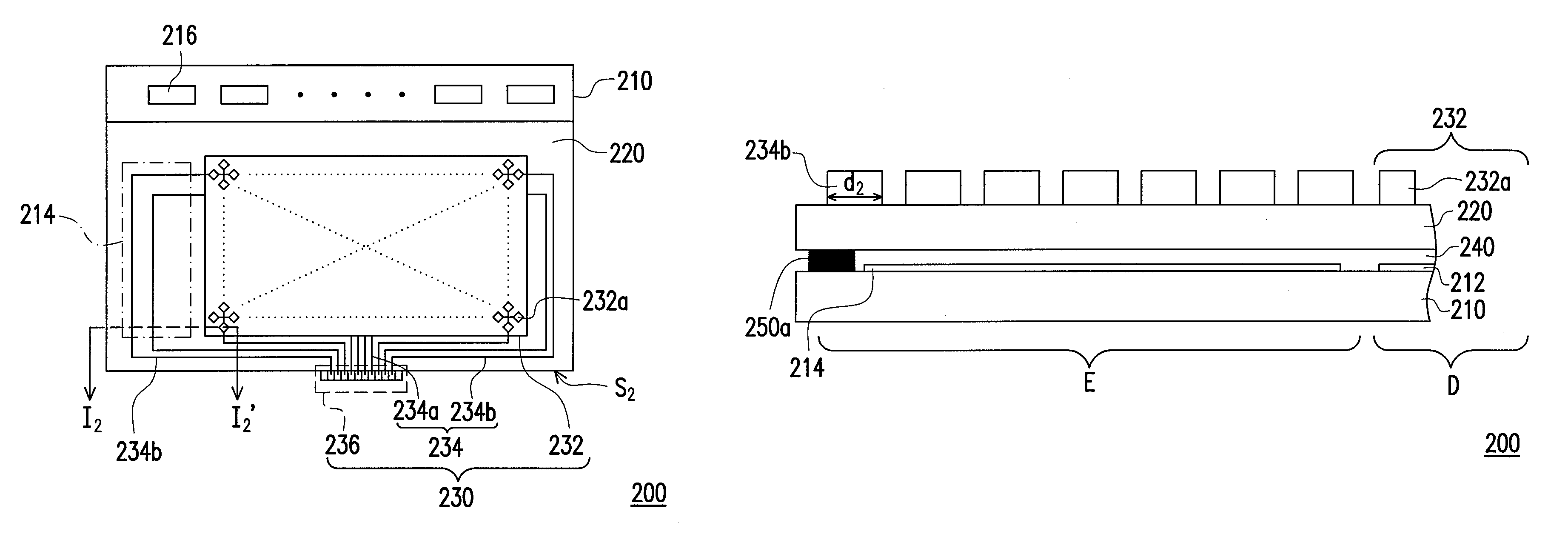
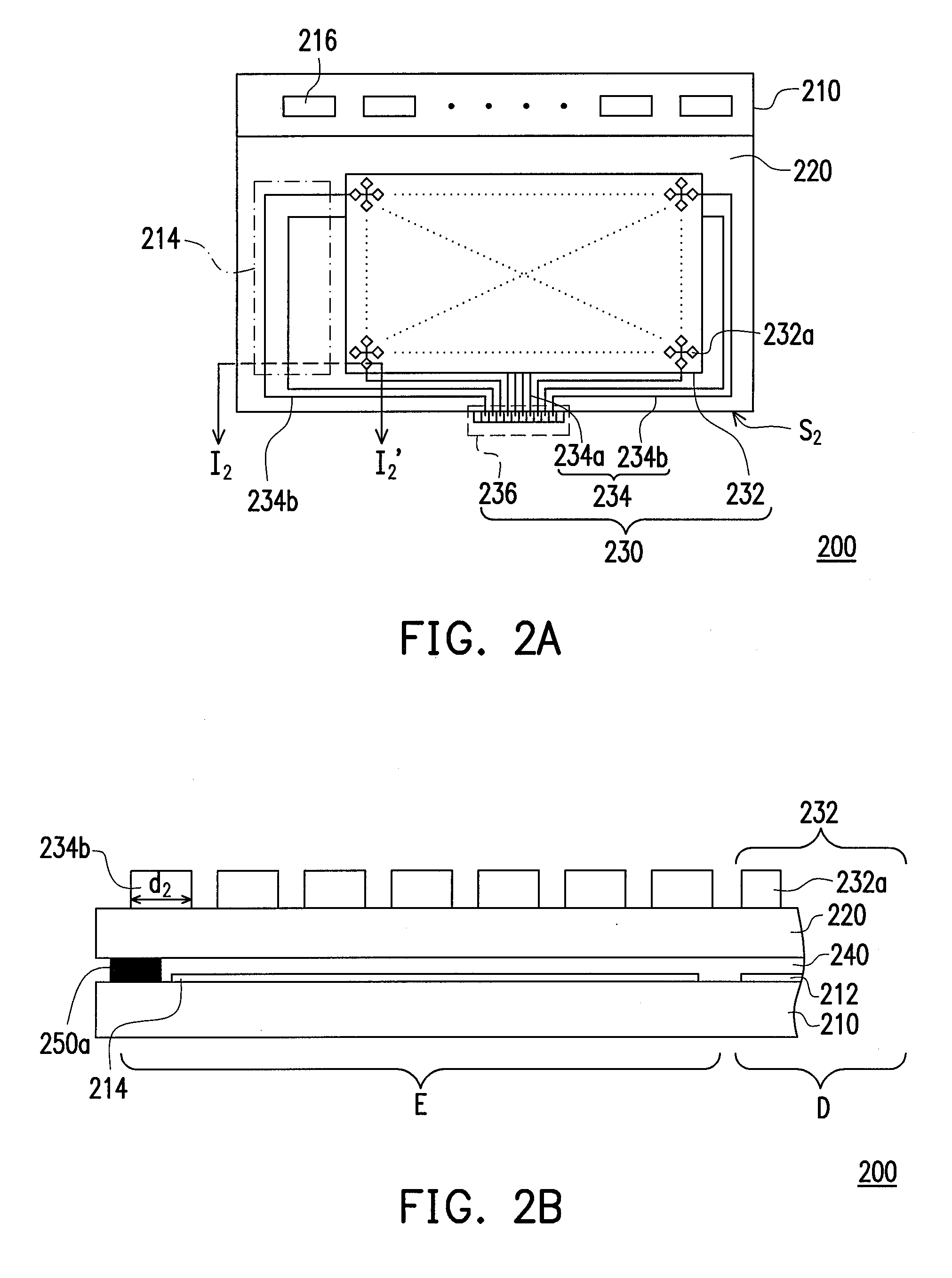
[0042]FIG. 2A is a top view of a touch panel display 200 according to the first embodiment of the present invention, and FIG. 2B and FIG. 2C are cross-sectional views of the touch panel display of FIG. 2A along a line I2-I2′. Referring to FIG. 2A and FIG. 2B, the touch panel display 200 of the present embodiment includes a first substrate 210, a second substrate 220, a touch device 230, a display medium 240 and a sealant 250a. A size of the first substrate 210 is greater than that of the second substrate 220. In detail, a width of the second substrate 220 is less than that of the first substrate 210, and a length of the second substrate 220 is substantially the same to that of the first substrate 210. Moreover, the sealant 250a and the two substrates 210 and 220 form a closed space to close the display medium 240 therein. In addition, the display medium 240 includes, for example, a liquid crystal layer, an organic light emitting material layer or an electrophoretic display material ...

second embodiment

[0053]FIG. 3A is a top view of a touch panel display 300 according to the second embodiment of the present invention, and FIG. 3B is a cross-sectional view of the touch panel display of FIG. 3A along a line I3-I3′. Referring to FIG. 3A and FIG. 3B, the touch panel display 300 of the present embodiment is similar to the touch panel display 200 of the first embodiment, and a difference there between is that the connecting terminal 236 of the present embodiment is located at a short side S3 of the second substrate 220. Namely, the wiring element 234 may protrude out pins at the short side S3 of the second substrate 220. In other words, as shown in FIG. 3B, the integrated driving circuit 214 is located between the pixel array 212 and the connecting terminal 236.

[0054]In detail, compared to the conventional driving circuit, since a thickness of the integrated driving circuit 214 of the present embodiment is relatively thin, the second substrate 220 can extend outside to cover at least a ...

third embodiment

[0055]FIG. 4A is a top view of a touch panel display 400 according to the third embodiment of the present invention, and FIG. 4B is a cross-sectional view of the touch panel display of FIG. 4A along a line I4-I4′. Referring to FIG. 4A and FIG. 4B, the touch panel display 400 of the present embodiment is similar to the touch panel display 300 of the second embodiment, and a difference there between is that the integrated driving circuit 214 of the touch panel display 400 of the present embodiment includes at least one GOA 214a and at least one SOA 214b. Therefore, the second substrate 220 can not only extend along the horizontal direction but can also extend along the vertical direction to respectively cover at least a portion of the GOA 214a and at least a portion of the SOA 214b. By such means, the space on the second substrate 220 that is used for configuring the wiring element 234 is larger than that of the first and the second embodiment, so that the quantity of the wiring eleme...


PUM


Abstract

A touch panel display including a first substrate, a second substrate, a display medium and a touch device is provided. The first substrate has a display area and a peripheral area. The first substrate has a pixel array in the display area and at least one integrated driving circuit in the peripheral area. The integrated driving circuit is electrically connected to the pixel array. The second substrate is disposed above the first substrate to cover the integrated driving circuit and the pixel array. The display medium is disposed on the pixel array and located between the first substrate and the second substrate. The touch device is disposed on the second substrate, and has a sensor element and a wiring element connected to the sensor element. The sensor element is located above the pixel array and the wiring element is located above at least a portion of the integrated driving circuit.

Description

CROSS-REFERENCE TO RELATED APPLICATION[0001]This application claims the priority benefit of Taiwan application serial no. 98117790, filed on May 27, 2009. The entirety of the above-mentioned patent application is hereby incorporated by reference herein and made a part of specification.BACKGROUND OF THE INVENTION[0002]1. Field of the Invention[0003]The present invention relates to a display. More particularly, the present invention relates to a touch panel display.[0004]2. Description of Related Art[0005]Recently, with quick development of information and wireless communication technologies and the widespread of various information products, the conventional input devices (for example, a keyboard or a mouse) of many information products have been replaced by touch panels in order to make these information products more convenient, compact, light-weighted, and personalized, wherein the touch panel is combined with a display to form a touch panel display. The touch panels of nowadays a...

Claims


Application Information

Patent Timeline
Patent Type & Authority Patents(United States)
IPC IPC(8): G06F3/041
CPCG06F3/041G06F3/0412G06F3/04164
Inventor LIU, PO-YUANLEE, HAO-CHIEHCHEN, CHIEN-LIANGKUO, CHUN-KU
Owner AU OPTRONICS CORP
Why Eureka
Try Eureka