Circuit substrate

a technology of circuit substrate and substrate layer, applied in the field of circuit substrate, can solve the problem that the grounding layer cannot be left out, and achieve the effect of increasing layout space, reducing inductance, and increasing q valu

Active Publication Date: 2005-07-14
ADVANCED SEMICON ENG INC
View PDF4 Cites 9 Cited by
  • Summary
  • Abstract
  • Description
  • Claims
  • Application Information

AI Technical Summary

Benefits of technology

[0009] It is therefore an object of the invention to provide a circuit substrate whose design of having an in-built inductor element not only increases the layout space but also produces a larger inductance value and a larger Q value.

Problems solved by technology

On the other hand, the grounding layer cannot be left out lest electromagnetism might be coupled to and interfere with adjacent elements.

Method used


Image

  • Circuit substrate
  • Circuit substrate
  • Circuit substrate

Examples


embodiment one

Preferred Embodiment One

[0024] Referring to FIG. 3A, a partial side sectional view of the micro-via of the circuit substrate according to preferred embodiment one of the invention is shown. The circuit substrate 300 has a first surface 314 and a second surface 316 corresponding to each other. The first micro-via 303 and the second micro-via 305 formed by the Laser cutting and drilling technique respectively penetrates to the second surface 316 through the first surface 314 of the circuit substrate 300.

[0025] Please refer to FIG. 3B, FIG. 3C and FIG. 3D together. FIG. 3B is a partial side sectional view of the circuit substrate according to preferred embodiment one of the invention; FIG. 3C is another partial side sectional view of the circuit substrate according to preferred embodiment one of the invention; and FIG. 3D is a partial three-dimensional diagram of the inductance of the circuit substrate according to preferred embodiment one of the invention.

[0026] The circuit substrat...

embodiment two

Preferred Embodiment Two

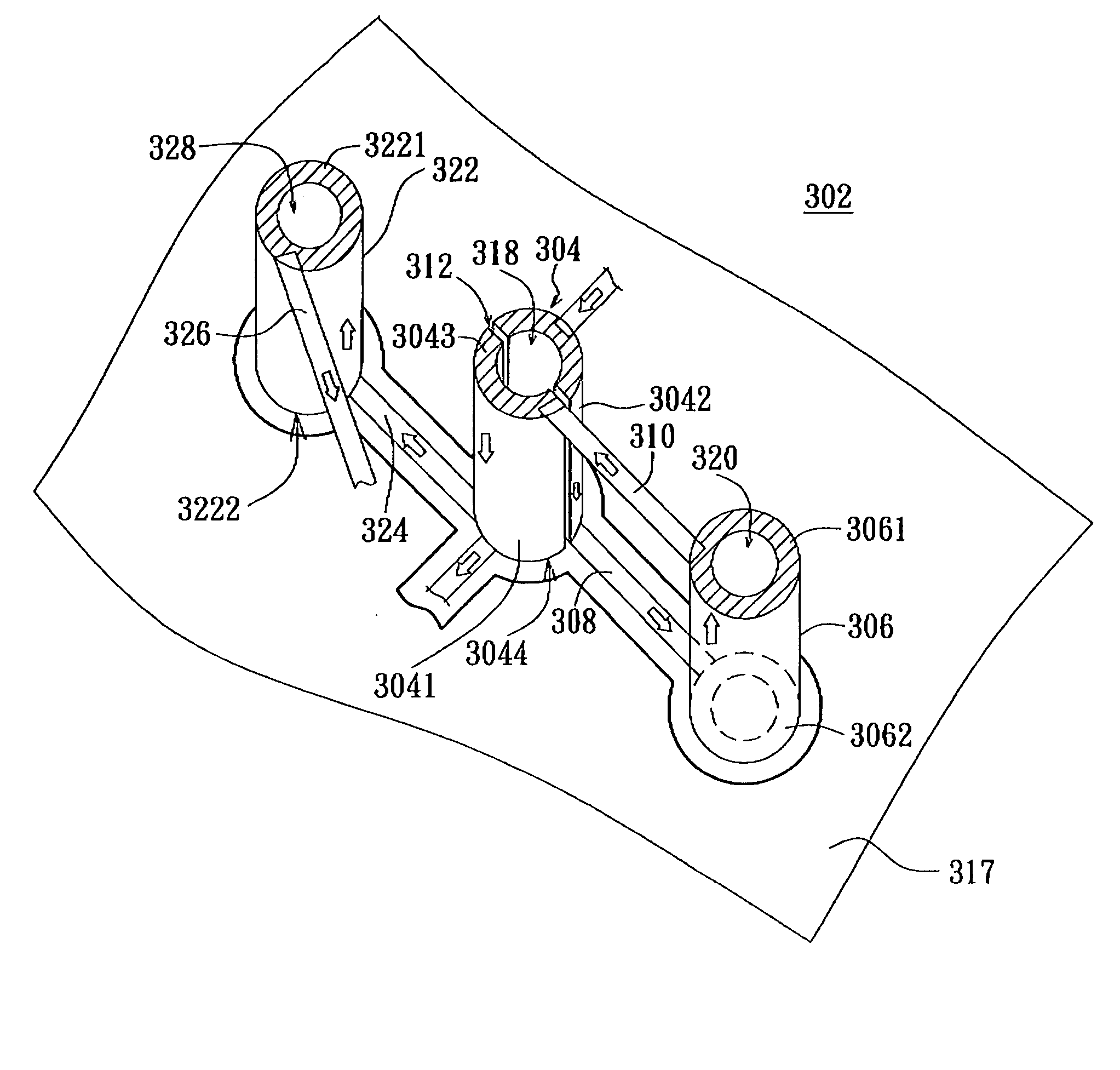
[0033] Referring to FIG. 4A, a top view of the micro-via array of the circuit substrate according to preferred embodiment two of the invention is shown. By means of a Laser cutting and drilling technique, a number of first micro-vias 403, second micro-vias 405, and third micro-vias 407 are respectively lined up on the substrate 402 in parallel.

[0034] Please refer to FIG. 4B and FIG. 4C together. FIG. 4B is a top view of the first surface of the circuit substrate according to preferred embodiment two of the invention; and FIG. 4C is a top view of the second surface of the circuit substrate according to preferred embodiment two of the invention.

[0035] The circuit substrate 400 comprises an inductor element 402 and a reference plane. The inductor element 302 mainly comprises a number of first conductive columns 404, the second conductive columns 406, the third conductive columns 408, the first traces 412 the second traces 414, the third traces 416, and the fou...


PUM

PropertyMeasurementUnit
diameteraaaaaaaaaa
diameteraaaaaaaaaa
conductiveaaaaaaaaaa

Abstract

A circuit substrate includes an inductor element and a reference plane. The inductor element includes a first conductive column, a second conductive column, a first trace, and a second trace. The first and second conductive columns penetrate the circuit substrate from a first surface to a corresponding second surface. The first conductive includes a left conductive column and a right conductive column. The second conductive column is adjacent to one side of the first conductive column. The first trace electrically connects a first lower portion of the left conductive column and a second lower portion of the second conductive column. The second trace electrically connects a first upper portion of the right conductive column and a second upper portion of the second conductive column. The reference plane is disposed on the second surface. Accordingly, the magnetic line of force produced by the inductor element is parallel to the reference plane.

Description

[0001] This application claims the benefit of Taiwan application Serial No. 93100723, filed Jan. 12, 2004, the subject matter of which is incorporated herein by reference. BACKGROUND OF THE INVENTION [0002] 1. Field of the Invention [0003] The invention relates in general to a circuit substrate, and more particularly to a circuit substrate using a Laser cutting and drilling technique to form a built-in inductor element. [0004] 2. Description of the Related Art [0005] Referring to FIG. 1A and FIG. 1B, a top view of a conventional spiral inductance and a side sectional view of a conventional spiral inductance are shown. Conventional spiral inductor 10, which is disposed on the surface of a substrate 14, is electrically connected with a grounding layer 16 through a micro-via 12. Magnetic line of force 18 is perpendicular to the grounding layer 16 and is reflected by the grounding layer 16 because the grounding layer 16 produces shielding effect to change the distribution of electrical ...

Claims


Application Information

Patent Timeline
Patent Type & Authority Applications(United States)
IPC IPC(8): G11C16/04H01F17/00H01L23/498H05K1/00H05K1/16
CPCH01F2017/002H01L23/49822H01L23/49827H05K1/165H05K2201/09645H01L2924/0002H05K2201/097H01L2924/00
Inventor CHIU, CHI-TSUNG
Owner ADVANCED SEMICON ENG INC
Why Eureka
Try Eureka