800G optical module

A technology of optical modules and lasers, which is applied in the field of optical communications, can solve the problems of low reliability of packaging methods, increased wiring density, and low reliability, and achieve the effects of avoiding too compact arrangement, good heat dissipation performance, and reducing crosstalk problems

Pending Publication Date: 2021-04-27
HENGTONG ROCKLEY TECHNOLOGY CO LTD
View PDF0 Cites 9 Cited by
  • Summary
  • Abstract
  • Description
  • Claims
  • Application Information

AI Technical Summary

Problems solved by technology

Due to the complexity of the current 800G optical module supporting circuit, there are many types and quantities of electronic components, and it is necessary to set avoidance or installation gaps on the PCB board during design. If the optical chip is packaged with the traditional COB solution, it will inevitably cause supporting circuits and Insufficient layout space for components, low PCB strength, high signal crosstalk, and low reliability
[0005] The existing 800G optical module supporting circuit is relatively complex, the types and quantities of components are various, the wiring density is increased, and the signal integrity problem is becoming more and more prominent. The current COB packaging process can no longer meet the demand, and most of them adopt the packaging method of BOX and flexible board.
The 800G optical module has a high transmission rate, a large transmission capacity, and a large number of electronic components and electrical interfaces. If the flexible board and the PCB are electrically connected by soldering, due to the limited space of the PCB layout, the width of the soldering pad cannot be low. If it is less than 0.2mm, the soldering yield cannot be guaranteed, so the reliability of this packaging method is low
If the flexible board and the PCB are electrically connected by gold wire bonding, although the reliability is improved to a certain extent, it still cannot effectively solve the problems of signal crosstalk and layout space.

Method used


Image

  • 800G optical module
  • 800G optical module
  • 800G optical module

Examples


Embodiment Construction

[0027] The technical solution of the present invention will be clearly and completely described below in conjunction with the accompanying drawings. The relevant components in the invention are not drawn according to the number, shape and size of the components in actual implementation. The type, quantity and proportion of each component in actual implementation can be changed arbitrarily, and the layout of the components may also be changed for complex.

[0028] The purpose of the present invention is to provide a packaging structure for 800G optical modules to address the shortcomings of the current optical module packaging structure, which not only ensures sufficient board space for optical module components and supporting circuits, but also ensures that optical chips The integrity of signal transmission and good heat dissipation performance, and the packaging structure is simple and reliable, and has good mass production feasibility.

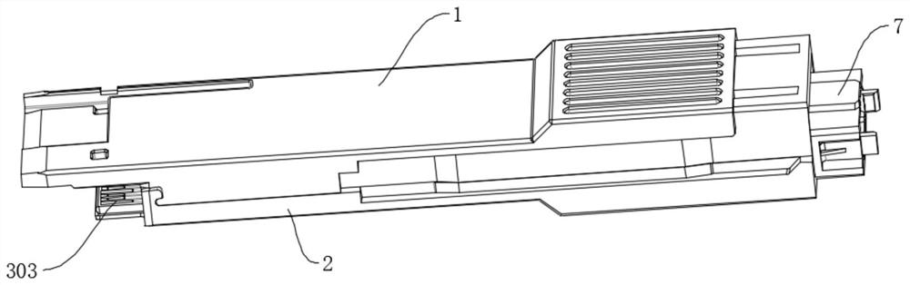
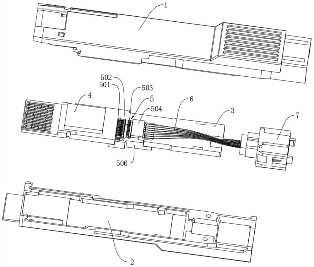
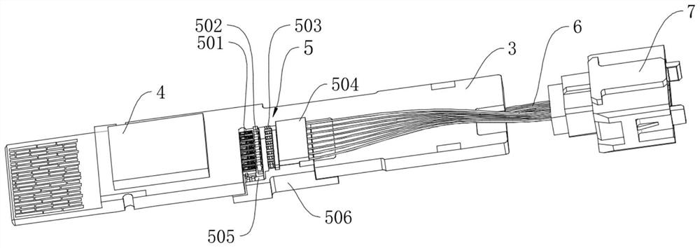
[0029] See Figure 1 to Figure 6 , ...


PUM


Abstract

The invention provides an 800G optical module, which is simple and reliable in structure, increases the layout space, avoids the over-compact arrangement of optical chips or circuits and greatly reduces the crosstalk between signals. The optical module comprises a main heat dissipation shell and an auxiliary heat dissipation shell which can be spliced into a whole, wherein an accommodating cavity is formed between the main heat dissipation shell and the auxiliary heat dissipation shell. An accommodating cavity is formed in the main heat dissipation shell, a PCB is arranged in the accommodating cavity, a control chip is arranged on the PCB, and the LED lamp is characterized in that the PCB comprises an electric port part and a thickening part, the electric port is formed in the electric port part, a transmitting end is arranged on one side, close to the main heat dissipation shell, of the thickening part of the PCB, and the transmitting end is connected to an optical port after being connected with an optical fiber. A receiving end is arranged on one side, close to the auxiliary heat dissipation shell, of the thickened part of the PCB, and the receiving end is connected to the optical port after being connected with an optical fiber.

Description

technical field [0001] The invention relates to the technical field of optical communication, in particular to an 800G optical module. Background technique [0002] With the continuous rapid development of my country's optical communication industry and the renewal and upgrading of communication technology, optical modules, as the basis for building modern high-speed information networks, play a central role in the optical communication industry, and their continuous development is an inevitable trend. The current development of optical modules is mainly manifested in high speed and high density. The transmission rate has ranged from 1.25G to 10G, 25G, 100G in the past, and now to 400G and 800G. The packaging method has changed from the original TO package to the COB package. From low-end to high-end, it is becoming more and more small-sized and high-density, and the development is rapid. [0003] As the rate requirements of optical modules are getting higher and higher, th...

Claims


Application Information

Patent Timeline
Patent Type & Authority Applications(China)
IPC IPC(8): G02B6/42
CPCG02B6/4245G02B6/4268G02B6/428
Inventor 尤炎炎梁巍王长江王志勇甘飞陈奔朱宇
Owner HENGTONG ROCKLEY TECHNOLOGY CO LTD
Why Eureka
Try Eureka