
Article management system
a management system and article technology, applied in the field of articles management systems, can solve the problems of one type of article that is easily lost, the article management system itself cannot function, and the loss of the interrogator itself cannot be prevented, so as to prevent the loss of articles, prevent the financial loss of users, and facilitate the management of articles.
- Summary
- Abstract
- Description
- Claims
- Application Information
AI Technical Summary
Benefits of technology
Problems solved by technology
Method used
Image

Examples
embodiment mode 1
(Embodiment Mode 1)
[0057]One aspect of an article management system to which the present invention is applied will be described with reference to drawings.
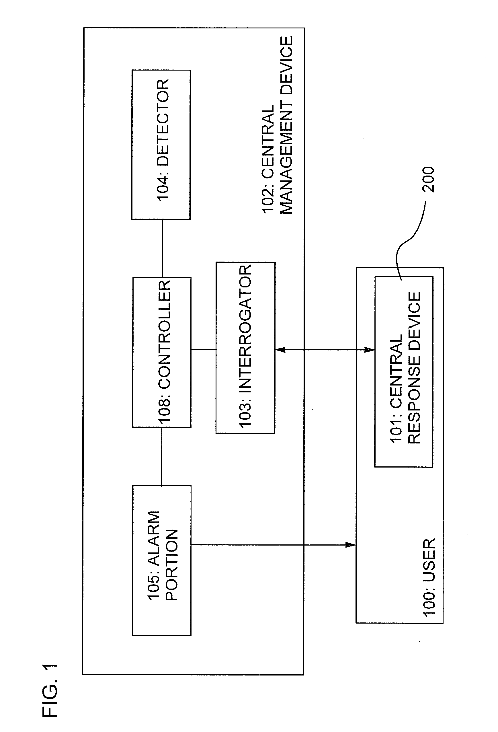
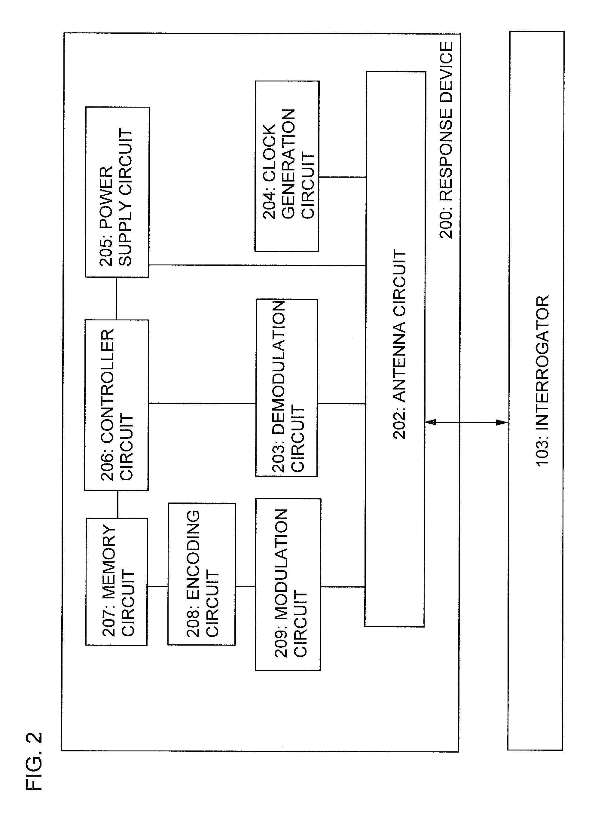
[0058]In FIG. 1, a block diagram used to describe a structure of an article management system of the present embodiment mode is shown. The article management system of the present embodiment mode has a central management device and a response device. The central management device has an interrogator, a detector, an alarm portion, and a controller. The response device has at least one central response device.
[0059]A user 100 is equipped with a central response device 101 and manages a central management device 102. The central response device 101 is provided separately from the central management device 102.
[0060]It is to be noted that the central response device 101 may be implanted directly into the user 100 or indirectly attached. Here, “indirectly attached” refers to a case in which the central response device 101 is attached t...
embodiment mode 2
(Embodiment Mode 2)
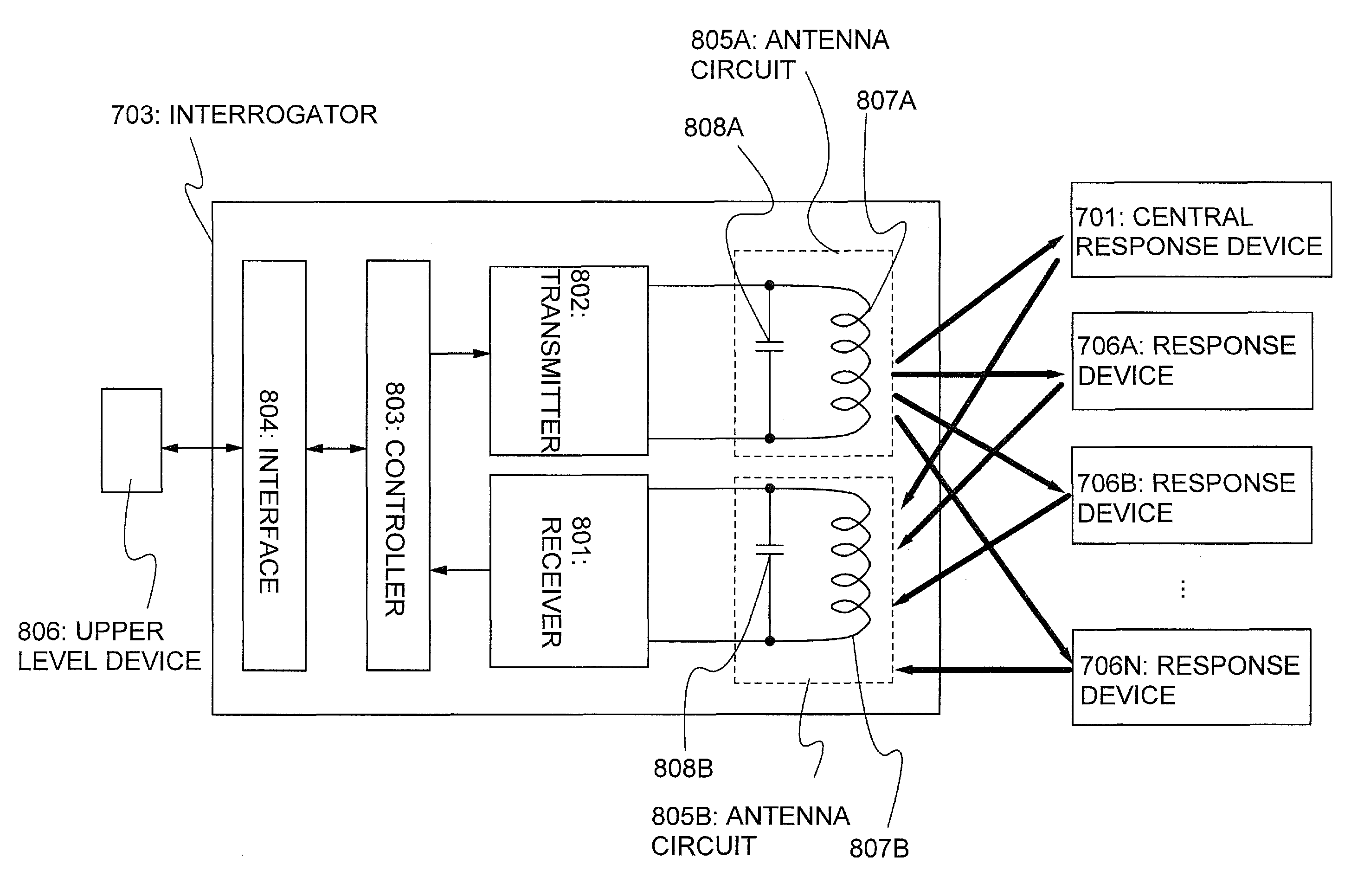
[0123]One aspect of an article management system to which the present invention is applied will be described with reference to FIG. 7, FIG. 8, and FIGS. 9A and 9B. In the present embodiment mode, an aspect, differing from that of Embodiment Mode 1, in which a response device is installed in each of a plurality of articles will be described.
[0124]In FIG. 7, a block diagram used to describe an article management system of the present embodiment mode is shown. The article management system of the present embodiment mode has a user, a central management device, a plurality of response devices, and a plurality of articles. The central management device has an interrogator, a detector, an alarm portion, and a controller. The response device has one central response device and a plurality of response devices that are installed in articles. Each of the plurality of response devices (a response device 706A, a response device 706B, and a response device 706N) is installed i...
embodiment mode 3
(Embodiment Mode 3)
[0164]In the present embodiment mode, an example of a manufacturing method for a semiconductor device used as the response device of the present invention will be described with reference to drawings. It is to be noted that, hereinafter, a case in which six thin film integrated circuits are formed over a substrate 111 will be described. In FIG. 15A, FIG. 16A, and FIG. 17A, a region in which one of the thin film integrated circuits is provided corresponds to a region 126 that is enclosed by a dotted line. FIG. 15B, FIG. 16B, and FIG. 17B are each diagrams of a cross section taken from point A to point B in FIG. 15A, FIG. 16A, and FIG. 17A, respectively.
[0165]First, an insulating layer 112 is formed over one surface of the substrate 111 (refer to FIG. 15B). Next, a layer that contains a plurality of transistors 113 is formed over the insulating layer 112. Then, an insulating layer 115 and an insulating layer 116 are formed over the layer that contains the plurality ...
PUM
 Abstract
Description
Claims
Application Information