Semiconductor memory device and programming method thereof

a semiconductor memory and three-dimensional technology, applied in static storage, digital storage, instruments, etc., can solve the problems of limited integration density of greatly affected conventional two-dimensional semiconductor memory devices, etc., and achieve high-reliability products.

Active Publication Date: 2013-04-23
SAMSUNG ELECTRONICS CO LTD
View PDF14 Cites 48 Cited by
  • Summary
  • Abstract
  • Description
  • Claims
  • Application Information

AI Technical Summary

Benefits of technology

[0006]Embodiments of the present general inventive concept provide three-dimensional semiconductor memory devices including memory cells arranged three-dimensionally. Embodiments of the present general inventive concept also provide methods of fabrication such that the cost per bit of three-dimensional semiconductor memory devices according to exemplary embodiments of the present inventive concept are lower than that of two-dimensional semiconductor memory devices. Exemplary embodiments of the present general inventive concept also provide control methods to control three-dimensionally arranged memory cell. Exemplary embodiments of the present general inventive concept provide methods and apparatus to control complex lines during a program operation of a three-dimensional semiconductor memory device to obtain highly reliable products.

Problems solved by technology

Therefore, the conventional two-dimensional semiconductor memory devices are greatly affected by fine-pattern forming technologies.
However, because extremely high-priced apparatuses are needed to achieve fine patterns, the integration density of two-dimensional semiconductor memory devices is still limited.

Method used


Image

  • Semiconductor memory device and programming method thereof
  • Semiconductor memory device and programming method thereof
  • Semiconductor memory device and programming method thereof

Examples


Embodiment Construction

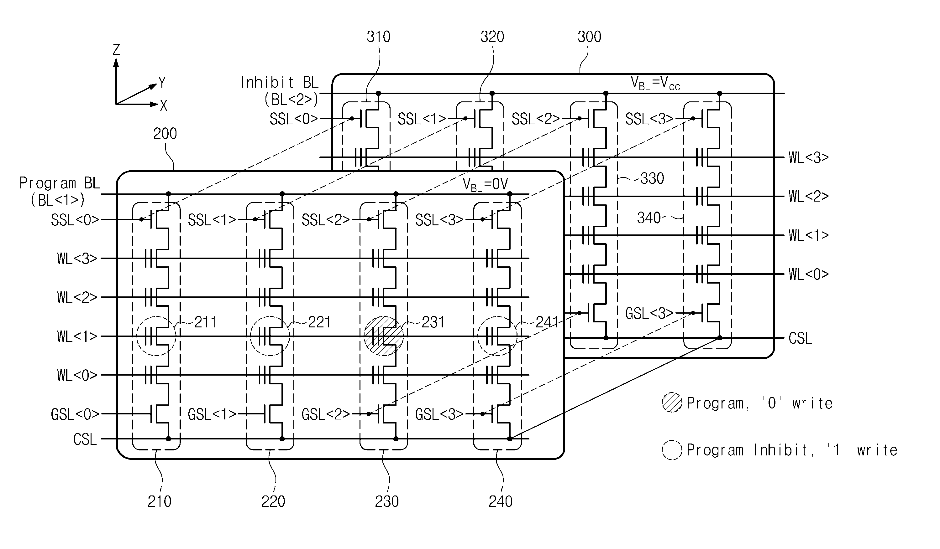
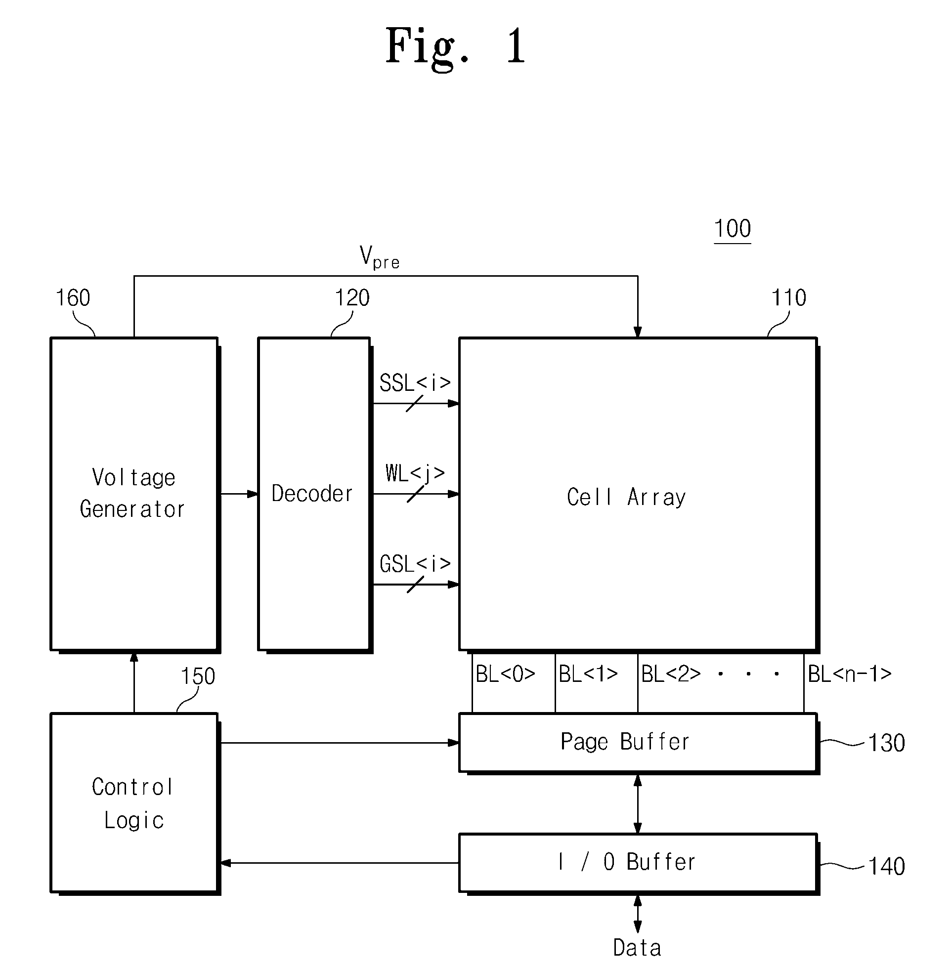
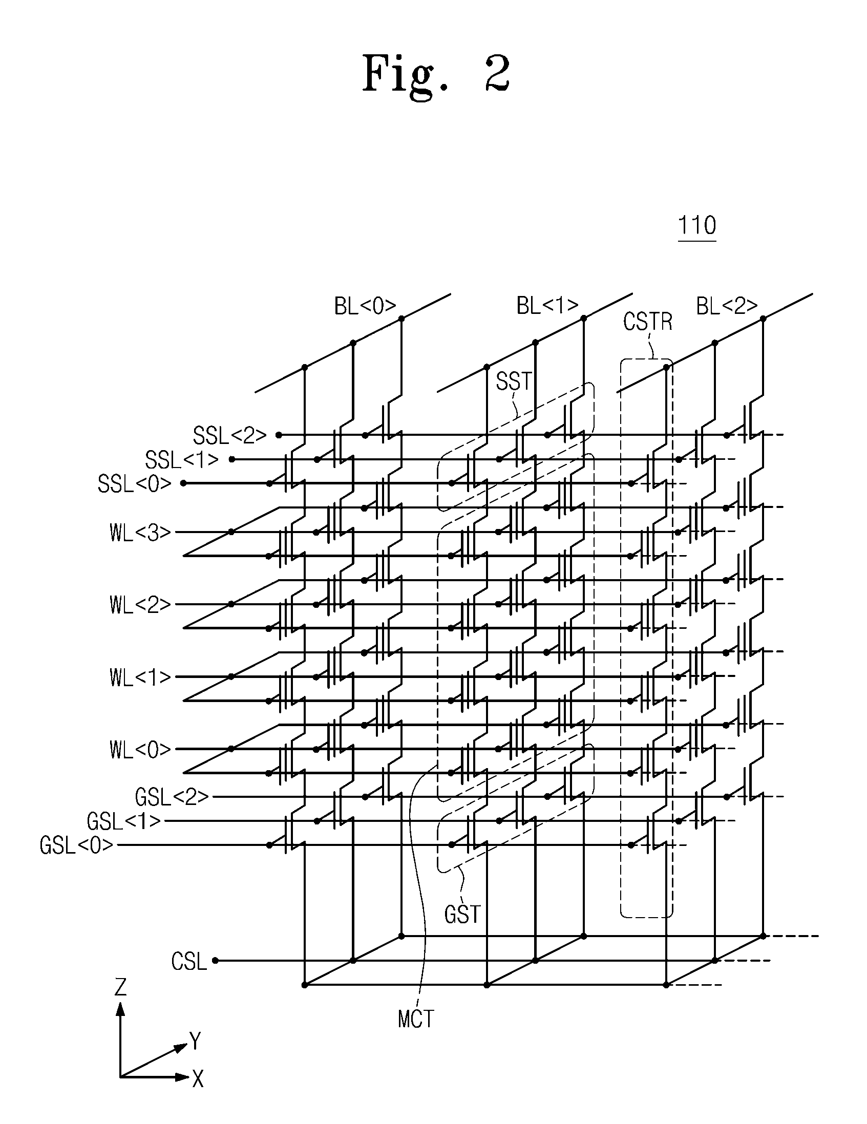
[0044]The present general inventive concept will now be described more fully hereinafter with reference to the accompanying drawings, in which exemplary embodiments of the present general inventive concept are illustrated. The present general inventive concept, however, may be embodied in many different forms and should not be construed as limited to the embodiments set forth herein. Rather, these embodiments are provided so that this disclosure will be thorough and complete, and will fully convey the scope of the invention to those skilled in the art. Like numbers refer to like elements throughout.

[0045]In the specification, the dimensions of layers and regions are exaggerated for clarity of illustration. It will also be understood that when a layer (or film) is referred to as being “on” another layer or substrate, it can be directly on the other layer or substrate, or intervening layers may also be present. Also, though terms like a first, a second, and a third are used to describ...


PUM


Abstract

A programming method of a semiconductor memory device includes charging a channel of an inhibit string to a precharge voltage provided to the common source line and boosting the charged channel by providing a wordline voltage to the cell strings. The inhibit string is connected to a program bitline among the bitlines.

Description

CROSS-REFERENCE TO RELATED APPLICATIONS[0001]This application claims priority under 35 U.S.C. §119 to Korean Patent Application No. 2009-0066933 filed on Jul. 22, 2009 in the Korean Intellectual Property Office (KIPO), the contents of which are herein incorporated by reference in their entirety.BACKGROUND[0002]1. Field of the Invention[0003]The present invention relates to semiconductor memory devices and, more specifically, to a three-dimensional semiconductor memory device and a programming method thereof.[0004]2. Description of the Related Art[0005]In order to meet ever-increasing needs of the users for superior performance and low costs, there is a requirement for high integration density of semiconductor memory devices. Since integration density of semiconductor memory devices is significant in determining the price of products, there is a requirement for increased integration density. In case of conventional two-dimensional semiconductor memory devices, their integration densi...

Claims


Application Information

Patent Timeline
Patent Type & Authority Patents(United States)
IPC IPC(8): G11C11/4094
CPCG11C16/0483G11C16/24G11C16/10
Inventor JANG, JAE HOONCHOI, JUNG DAL
Owner SAMSUNG ELECTRONICS CO LTD
Why Eureka
Try Eureka