Layered chip package

a chip and chip technology, applied in the field of layered chip packages, can solve the problems of affecting the acceleration of circuit operation, difficulty in reducing the distance between the electrodes, and affecting the operation of the circuit, so as to reduce the problems attributable, and disable the use of malfunctioning chips

Inactive Publication Date: 2013-06-18
HEADWAY TECH INC +1
View PDF11 Cites 0 Cited by
  • Summary
  • Abstract
  • Description
  • Claims
  • Application Information

AI Technical Summary

Benefits of technology

[0013]It is an object of the present invention to provide a layered chip package and a method of manufacturing the same, the layered chip package including a plurality of chips stacked and being capable of disabling the use of a malfunctioning chip while reducing the problems attributable to the circuit in the malfunctioning chip.
[0023]According to the layered chip package or its manufacturing method of the present invention, it is possible to disable the use of a malfunctioning chip while reducing the problems attributable to the circuit in the malfunctioning chip.

Problems solved by technology

The wire bonding method has the problem that it is difficult to reduce the distance between the electrodes so as to avoid contact between wires, and the problem that the high resistances of the wires hinder the acceleration of operation of circuits.
Assume, however, that a chip including a control circuit and a plurality of memory cells has become defective due to, for example, a wiring failure of the control circuit, and it does not function normally even by employing the redundancy technique.
In such a case, the defective chip is no longer usable.
While the defective chip can be replaced with a conforming one, it increases the cost for the layered chip package.
In the case of a layered chip package formed using the through electrode method, however, disabling a defective chip produces the following problem.
In such a case, the circuit in the defective chip can produce capacitances and inductances that are unnecessary for a device to be implemented by the layered chip package, such as a memory device.
This hinders the acceleration of operation of the device such as a memory device.

Method used


Image

  • Layered chip package
  • Layered chip package
  • Layered chip package

Examples


first embodiment

[First Embodiment]

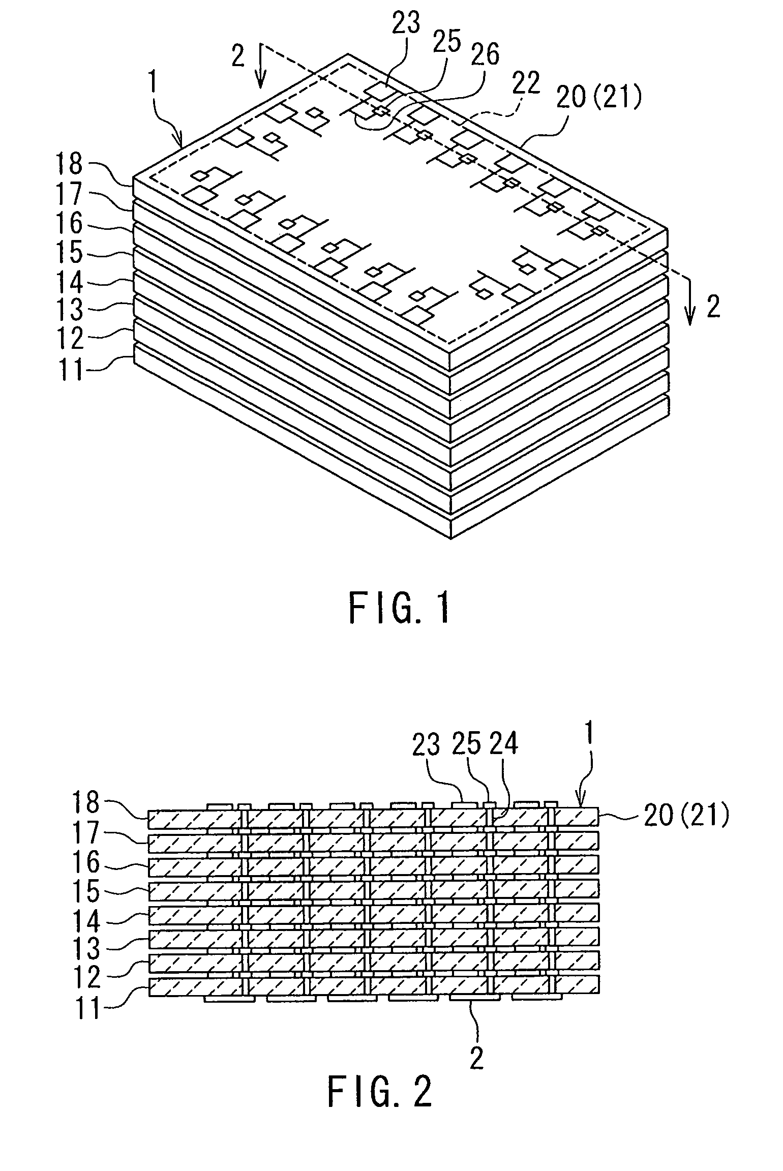
[0048]Preferred embodiments of the present invention will now be described in detail with reference to the drawings. Reference is first made to FIG. 1 and FIG. 2 to describe the configuration of a layered chip package according to a first embodiment of the invention. FIG. 1 is a perspective view of the layered chip package according to the present embodiment. FIG. 2 shows a cross section taken along line 2-2 of FIG. 1.

[0049]As shown in FIG. 1 and FIG. 2, the layered chip package 1 according to the present embodiment includes a plurality of layer portions stacked. Each of the layer portions includes a semiconductor chip 20. By way of example, FIG. 1 and FIG. 2 show a case where the layered chip package 1 includes eight layer portions 11, 12, 13, 14, 15, 16, 17 and 18 which are stacked in this order from the bottom. The number of layer portions to be included in the layered chip package 1 is not limited to eight, however, and may be any number that is no smaller than...

second embodiment

[Second Embodiment]

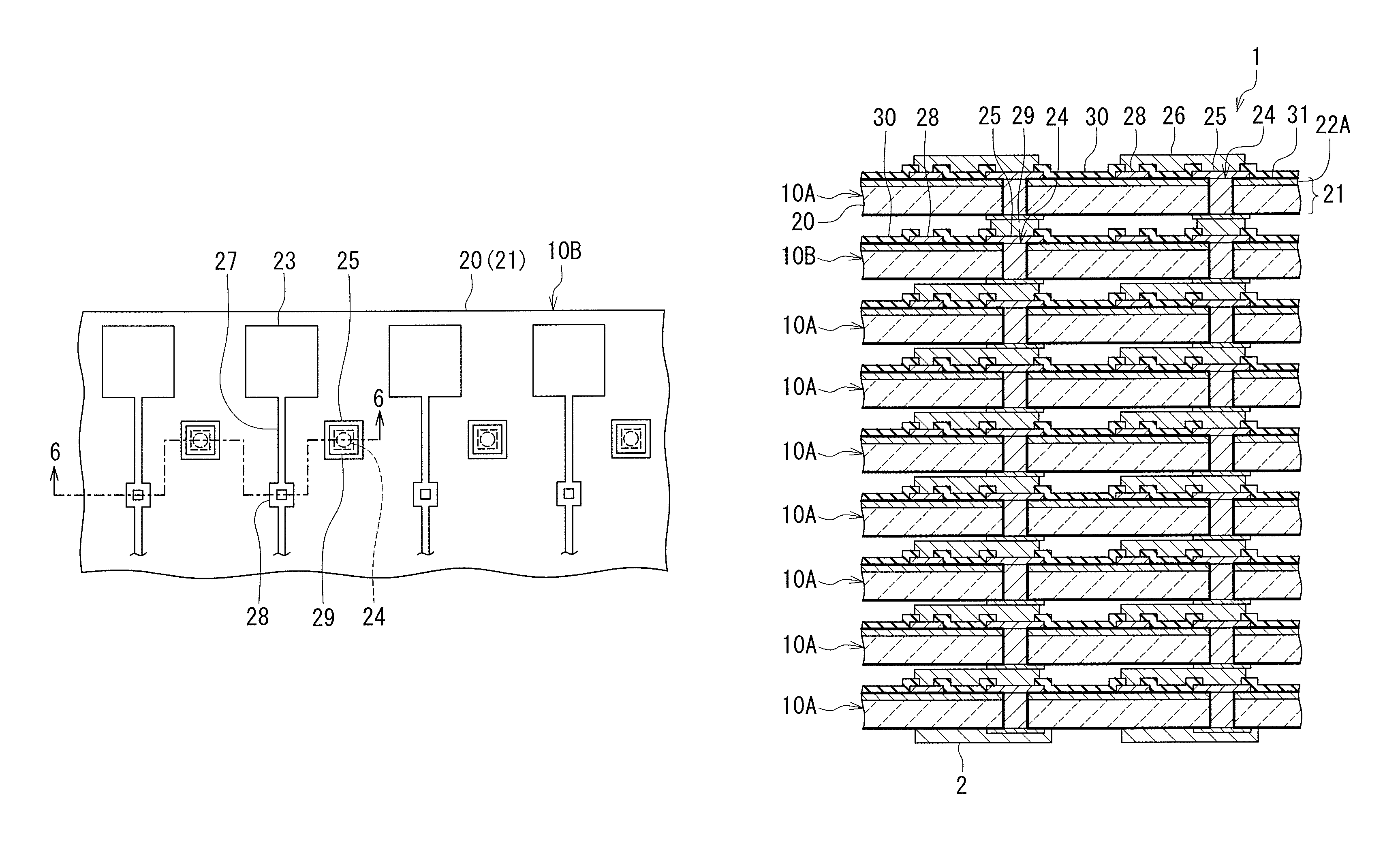
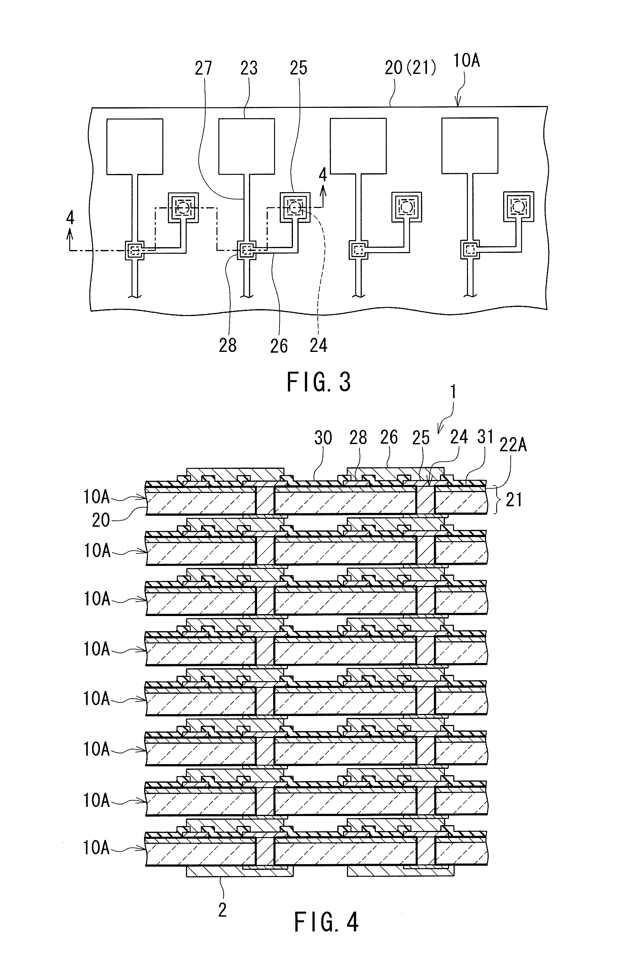
[0109]A layered chip package 1 and its manufacturing method according to a second embodiment of the invention will now be described. Reference is now made to FIG. 19 and FIG. 20 to describe the configuration of the layered chip package 1 according to the present embodiment. FIG. 19 is a plan view showing a part of the second-type layer portion 10B. FIG. 20 is a cross-sectional view showing a part of the layered chip package 1 that includes the first-type layer portion 10A and the second-type layer portion 10B. The cross section of the second-type layer portion 10B shown in FIG. 20 is taken along line 20-20 of FIG. 19. The cross section of the first-type layer portions 10A shown in FIG. 20 is taken along line 4-4 of FIG. 3.

[0110]In the layered chip package 1 according to the present embodiment, the first-type layer portion 10A has the same configuration as in the first embodiment. The second-type layer portion 10B of the present embodiment includes a plurality of c...


PUM


Abstract

A layered chip package includes a plurality of layer portions that are stacked, each of the layer portions including a semiconductor chip. The plurality of layer portions include at least one first-type layer portion and at least one second-type layer portion. The semiconductor chip has a circuit, a plurality of electrode pads electrically connected to the circuit, and a plurality of through electrodes. In every vertically adjacent two of the layer portions, the plurality of through electrodes of the semiconductor chip of one of the two layer portions are electrically connected to the respective corresponding through electrodes of the semiconductor chip of the other of the two layer portions. The first-type layer portion includes a plurality of wires for electrically connecting the plurality of through electrodes to the respective corresponding electrode pads, whereas the second-type layer portion does not include the wires.

Description

BACKGROUND OF THE INVENTION[0001]1. Field of the Invention[0002]The present invention relates to a layered chip package that includes a plurality of chips stacked and a method of manufacturing the same.[0003]2. Description of the Related Art[0004]In recent years, a reduction in weight and an improvement in performance have been demanded of mobile devices typified by cellular phones and notebook personal computers. Accordingly, there has been a demand for higher integration of electronic components for use in mobile devices. Higher integration of electronic components has been demanded also for achieving an increase in capacity of semiconductor memory.[0005]As an example of highly integrated electronic components, a system-in-package (hereinafter referred to as SiP), especially an SiP utilizing a three-dimensional packaging technology for stacking a plurality of semiconductor chips, has attracting attention in recent years. In the present application, a package that includes a plural...

Claims


Application Information

Patent Timeline
Patent Type & Authority Patents(United States)
IPC IPC(8): H01L23/48
CPCH01L23/481H01L24/11H01L24/94H01L25/0657H01L25/50H01L2924/0002H01L2224/0557H01L2224/1147H01L2224/13099H01L2225/06513H01L2225/06541H01L2225/06596H01L2924/01078H01L2924/01082H01L2924/3025H01L2924/01005H01L2924/01006H01L2924/01033H01L2924/014H01L2224/05554H01L2224/0401H01L2224/05552H01L24/05
Inventor SASAKI, YOSHITAKAITO, HIROYUKIIKEJIMA, HIROSHIIIJIMA, ATSUSHI
Owner HEADWAY TECH INC
Why Eureka
Try Eureka