Stackable molded microelectronic packages

a technology of microelectronic packages and molded parts, which is applied in the direction of semiconductor devices, semiconductor/solid-state device details, electrical apparatuses, etc., can solve the problems of imposing stress on assemblies including packages, terminals moving relative to the contact, and imposing stress on solders

Active Publication Date: 2013-07-09
TESSERA INC
View PDF379 Cites 113 Cited by
  • Summary
  • Abstract
  • Description
  • Claims
  • Application Information

AI Technical Summary

Problems solved by technology

Assemblies including packages can suffer from stresses imposed by differential thermal expansion and contraction of the device and the substrate.
Where the terminals of the package are fixed relative to the chip or other device, such as by using solder, these effects tend to cause the terminals to move relative to the contact pads on the circuit board.
This can impose stresses in the solder that connects the terminals to the contact pads on the circuit board.
Testing of packaged devices poses another formidable problem.
However, it is difficult to make connections by pressing the package against a simple test fixture such as an ordinary circuit board having planar contact pads.
For example, in a BGA package, differences in the diameter of the solder balls attached to the terminals, and non-planarity of the chip carrier, may cause some of the solder balls to lie at different heights.
However, such features add to the cost of the test fixture and, in some cases, introduce some unreliability into the test fixture itself.
This is particularly undesirable because the test fixture, and the engagement of the device with the test fixture, should be more reliable than the packaged devices themselves in order to provide a meaningful test.
This requirement imposes constraints on the electrical characteristics of the signal paths in the test fixture, which further complicates construction of the test fixture.
Additionally, when testing packaged devices having solder balls connected with terminals, solder tends to accumulate on those parts of the test fixture that engage the solder balls.
This accumulation of solder residue can shorten the life of the test fixture and impair its reliability.

Method used


Image

  • Stackable molded microelectronic packages
  • Stackable molded microelectronic packages
  • Stackable molded microelectronic packages

Examples


Embodiment Construction

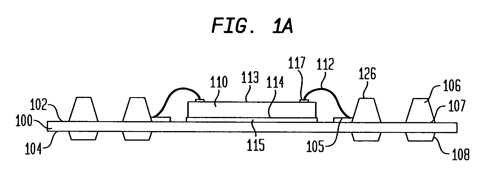
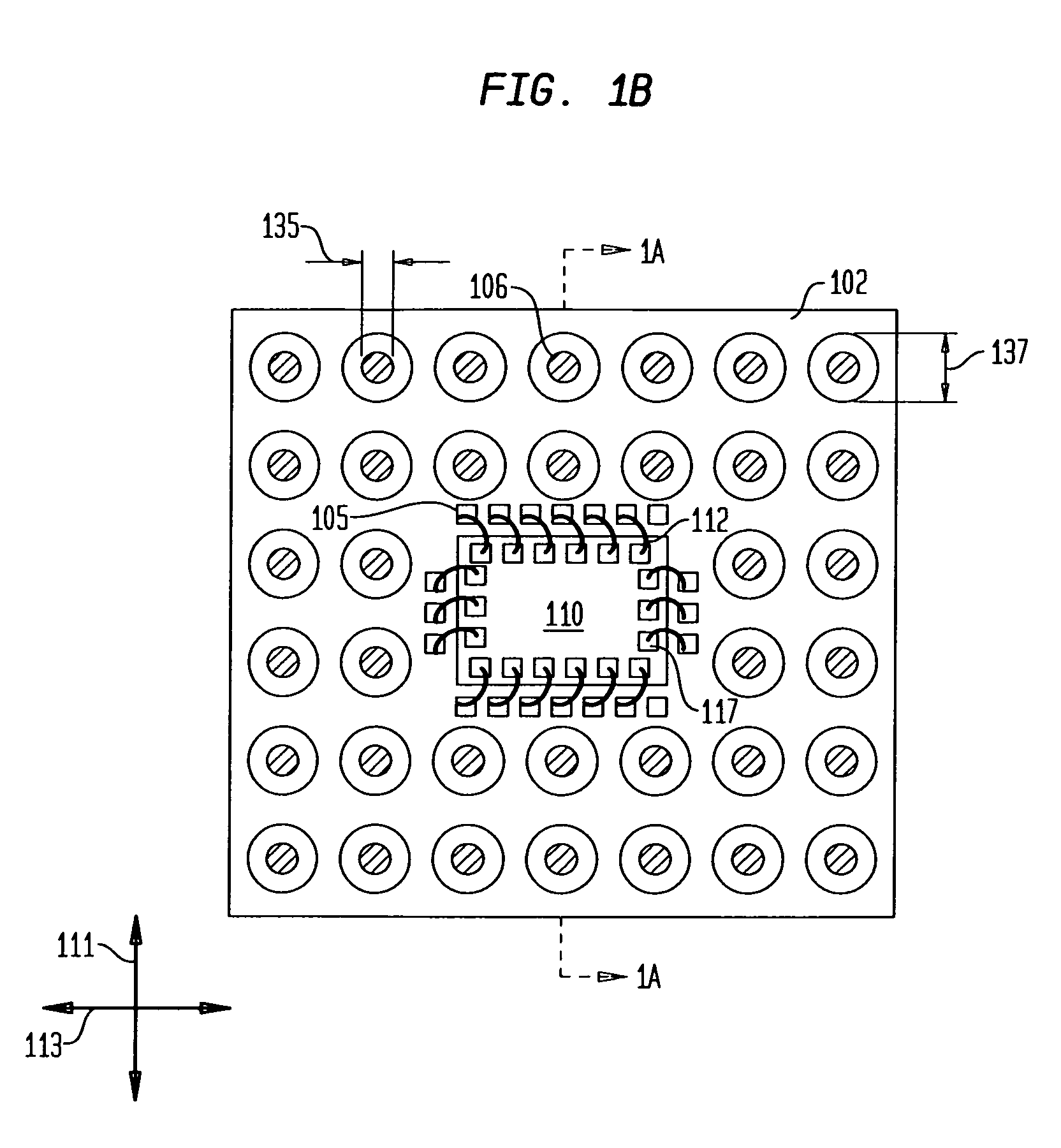
[0053]Referring to FIG. 1A, in accordance with an embodiment of the present invention, a microelectronic package includes a substrate 100 having a first or top surface 102 adjacent a face 114 of a microelectronic element 110 and a second or bottom surface 104 opposite therefrom. The microelectronic element 110 can be a first semiconductor chip having a front face 113 facing in an upward direction toward the top of the drawing in FIG. 1A and a rear face 114 facing in the opposite, rearward direction. Rear face 114 is generally parallel to front face 113. The directions parallel to front face 113 are referred to herein as “horizontal” or “lateral” directions; whereas the directions perpendicular to the front face are referred to herein as upward or downward directions and are also referred to herein as the “vertical” directions. The directions referred to herein are in the frame of reference of the structures referred to. Thus, these directions may lie at any orientation to the normal...


PUM


Abstract

A microelectronic package has a microelectronic element overlying or mounted to a first surface of a substrate and substantially rigid conductive posts projecting above the first surface or projecting above a second surface of the substrate remote therefrom. Conductive elements exposed at a surface of the substrate opposite the surface above which the conductive posts project are electrically interconnected with the microelectronic element. An encapsulant overlies at least a portion of the microelectronic element and the surface of the substrate above which the conductive posts project, the encapsulant having a recess or a plurality of openings each permitting at least one electrical connection to be made to at least one conductive post. At least some conductive posts are electrically insulated from one another and adapted to simultaneously carry different electric potentials. In particular embodiments, the openings in the encapsulant at least partially expose conductive masses joined to posts, fully expose top surfaces of posts and partially expose edge surfaces of posts, or may only partially expose top surfaces of posts.

Description

FIELD OF THE INVENTION[0001]The present invention relates to microelectronic packages and to methods of making or testing microelectronic packages.BACKGROUND OF THE INVENTION[0002]Microelectronic devices such as semiconductor chips typically require many input and output connections to other electronic components. The input and output contacts of a semiconductor chip or other comparable device are generally disposed in grid-like patterns that substantially cover a surface of the device (commonly referred to as an “area array”) or in elongated rows which may extend parallel to and adjacent each edge of the device's front surface, or in the center of the front surface. Typically, devices such as chips must be physically mounted on a substrate such as a printed circuit board, and the contacts of the device must be electrically connected to electrically conductive features of the circuit board.[0003]Semiconductor chips are commonly provided in packages that facilitate handling of the ch...

Claims


Application Information

Patent Timeline
Patent Type & Authority Patents(United States)
IPC IPC(8): H01L23/31H01L23/498H01L25/10H01L21/56
CPCH01L21/565H01L23/49811H01L25/105H01L23/3128H01L23/3157H01L24/14H01L2224/1401H01L2224/48091H01L2224/48227H01L2224/73265H01L2225/06565H01L2924/15311H01L2924/1815H01L2225/1058H01L2225/1023H01L2224/32145H01L2224/32225H01L24/48H01L2924/00014H01L2924/00012H01L2924/181H01L2924/12042H01L24/73H01L2224/05554H01L2924/10161H01L2224/48145H01L25/0657H01L2225/0651H01L2225/1047H01L2924/00H01L2224/45099H01L2224/45015H01L2924/207H01L2224/05599H01L2224/85399H01L23/28H01L23/12H01L24/16H01L21/56H01L23/3121H01L23/49838H01L2225/06517H01L23/315H01L23/49805H01L25/50H01L2224/48106H01L2225/0652H01L2225/06548H01L2225/06572
Inventor HABA, BELGACEM
Owner TESSERA INC
Why Eureka
Try Eureka