Method for smoothing group III nitride semiconductor substrate
a nitride semiconductor and nitride technology, applied in semiconductor/solid-state device manufacturing, basic electric elements, electric devices, etc., can solve the problems of tedious yellow light process, limited bowing reduction and inability to measure the bowing phenomenon of free-standing gan substrates in time for flexible adjustment, so as to reduce the bowing phenomenon of convex or concave, reduce the bowing phenomenon of free-standing gan substra
- Summary
- Abstract
- Description
- Claims
- Application Information
AI Technical Summary
Benefits of technology
Problems solved by technology
Method used
Image

Examples
embodiment 1
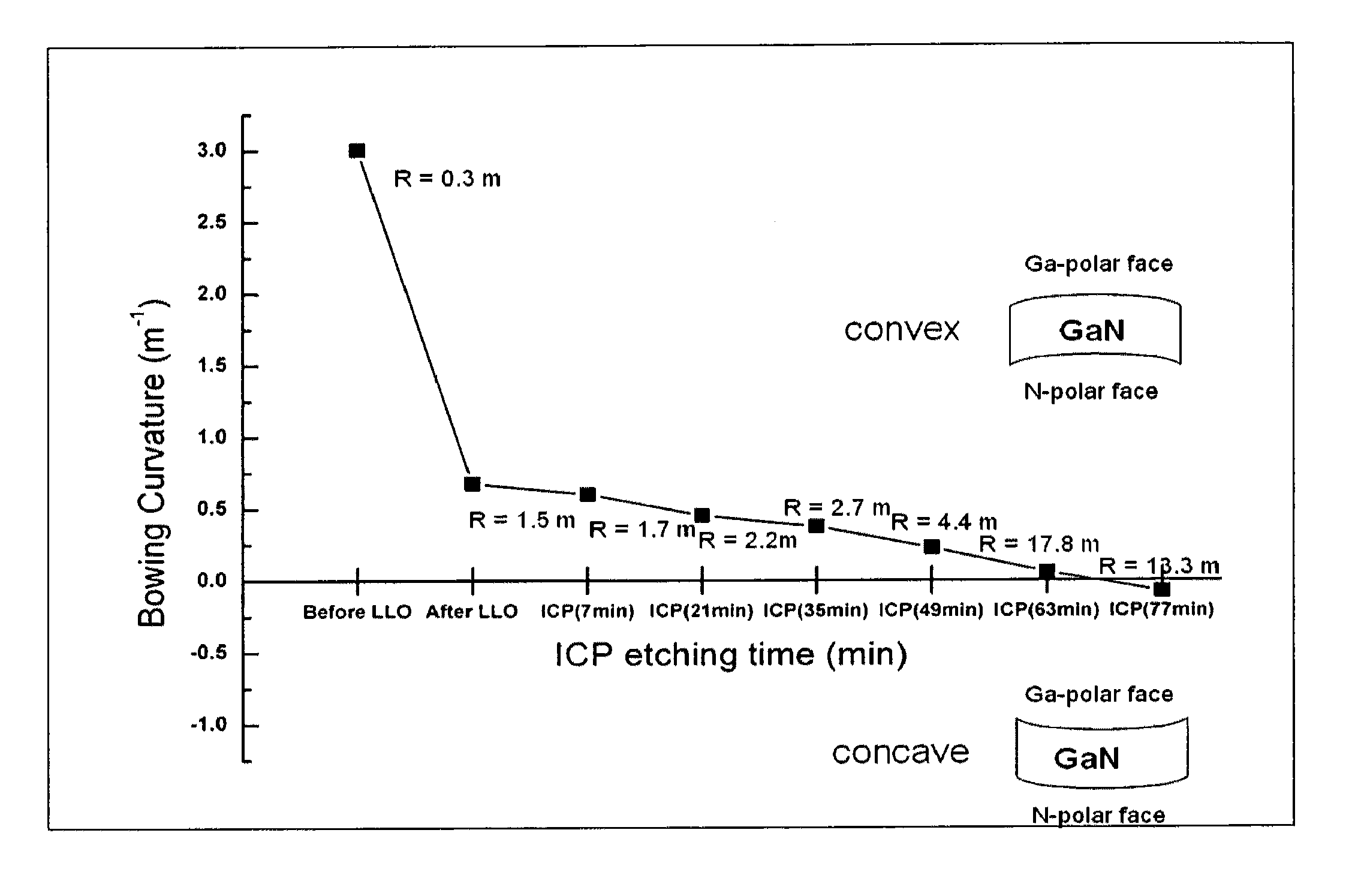
[0033]The invention discloses a method for smoothing a group III nitride semiconductor substrate. Firstly, the convex gallium nitride (GaN) substrate is provided. The reaction coupling plasma ion technology (dry etching technology) is used to etch the bottom of free-standing gallium nitride substrate. The chlorine (Cl2) and argon (Ar) are used as the etching gases. The first etching time is 7 minutes for the first time. The follow-up etching time is accumulated by 14 minutes every time. It means the etching time is 21 minutes for the second time, 35 minutes for the third time, 49 minutes for the fourth time, 63 minutes for the fifth time, and 77 minutes for the fifth time and so on.
[0034]Measure the bowing radius of convex gallium nitride before and after every etching process. The relation of bowing radius versus etching time is shown in FIG. 1. In the FIG. 1, the bowing curvature is defined as the inverse of bowing radius. When the bowing curvature is smaller, the bowing radius is...
embodiment 2
[0039]The invention discloses a method for smoothing a group III nitride semiconductor substrate. Firstly, the concave free-standing gallium nitride substrate is provided. The reaction coupling plasma ion technology (dry etching technology) is used to etch the top of free-standing GaN substrate. The chlorine and argon are used as the etching gases. The etching time is 7 minutes for the first time. The follow-up etching time is accumulated by 14 minutes every time. It means the etching time is 21 minutes for the second time, 35 minutes for the third time, and 49 minutes for the fourth time and so on.
[0040]Measure the bowing radius of concave free-standing gallium nitride before and after every etching process. The relation of bowing radius versus etching time is shown in FIG. 5. It is observed that the bowing radius is changed from 2.8 m and is become larger with the etching time. When the etching time is 49 minutes, the bowing radius is 15.0 m, and the bowing phenomenon is almost di...
embodiment 3
[0044]The invention discloses a method for smoothing a group III nitride semiconductor substrate. FIG. 8A shows the side view of convex free-standing GaN substrate 801 after the etching process. Firstly, the convex free-standing GaN substrate 801 is provided, and sputtering (or depositing) a dielectric layer (or metal layer) 802 on a top of the convex free-standing GaN substrate 801. The wet etching (or electrochemical etching) method is used to etch the bottom of convex free-standing GaN substrate 801. Finally, the above-mentioned dielectric layer (or metal layer) 802 is removed.
[0045]Also, FIG. 8A shows the side view of convex free-standing GaN substrate 801 after etching. The rod-type structure, hole-type structure, or flat-type structure 803 on convex free-standing GaN substrate 801 will release the stress on convex free-standing GaN substrate 801, so that the bowing level will be decreased gradually.
[0046]The invention discloses a smoothing method to decrease bowing of group II...
PUM
| Property | Measurement | Unit |
|---|---|---|
| bowing radius | aaaaa | aaaaa |
| bowing radius | aaaaa | aaaaa |
| bowing radius | aaaaa | aaaaa |
Abstract
Description
Claims
Application Information
 - R&D Engineer
- R&D Manager
- IP Professional
- Industry Leading Data Capabilities
- Powerful AI technology
- Patent DNA Extraction
Browse by: Latest US Patents, China's latest patents, Technical Efficacy Thesaurus, Application Domain, Technology Topic.
© 2024 PatSnap. All rights reserved.Legal|Privacy policy|Modern Slavery Act Transparency Statement|Sitemap