Gallium nitride based semiconductor device and method of manufacturing the same

a technology of gallium nitride and semiconductors, applied in semiconductor/solid-state device manufacturing, semiconductor devices, electrical equipment, etc., can solve the problems of increasing the bow of the wafer itself, many defects may occur on the grown gan thin film, and damage to the wafer. , to achieve the effect of enhancing the uniformity of wavelengths of light emitted, reducing the bow of the wafer, and reducing damage and deformation of the wafer

Active Publication Date: 2015-12-01
SAMSUNG ELECTRONICS CO LTD
View PDF11 Cites 2 Cited by
  • Summary
  • Abstract
  • Description
  • Claims
  • Application Information

AI Technical Summary

Benefits of technology

[0008]Example embodiments provide gallium nitride based semiconductor devices that simultaneously reduce damage and deformation of a wafer and enhance uniformity of wavelengths of light emitted by reducing a bow of the wafer, and methods of manufacturing the same.

Problems solved by technology

However, GaN thin films are grown on heterogeneous substrates, e.g., sapphire, SiC and / or Si, due to absence of homogeneous substrates.
As a result, many defects may occur on grown GaN thin films due to a mismatch in lattice constants between GaN thin films and heterogeneous substrates.
Also, a bow of a wafer itself increases due to a mismatch in thermal expansion coefficients between GaN thin films and heterogeneous substrates.
If the mismatch increases, cracks may occur in GaN thin films, or heterogeneous substrates may be broken.
However, because silicon substrates become ductile at a relatively high temperature, such a relatively high temperature and relatively high compressive stress may cause a plastic deformation of silicon substrates.
As a result, silicon substrates after being cooled may have relatively large bows in convex shapes and be hardened or broken.
Such a large bow of a substrate causes temperature non-uniformity during an MQW growth process, which causes a non-uniform composition of In in the MQW.
Thus, wavelengths of light generated in the MQW are not uniform, which may deteriorate a yield of an LED.
However, an increase in a substrate thickness may raise the price of a substrate as well as may not completely prevent or reduce a plastic deformation of a silicon substrate at a relatively high temperature.

Method used


Image

  • Gallium nitride based semiconductor device and method of manufacturing the same
  • Gallium nitride based semiconductor device and method of manufacturing the same
  • Gallium nitride based semiconductor device and method of manufacturing the same

Examples


Embodiment Construction

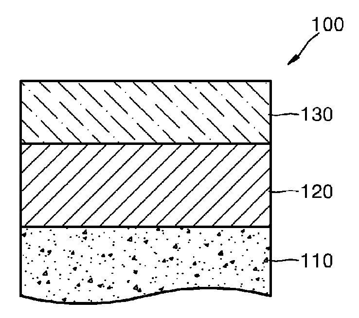
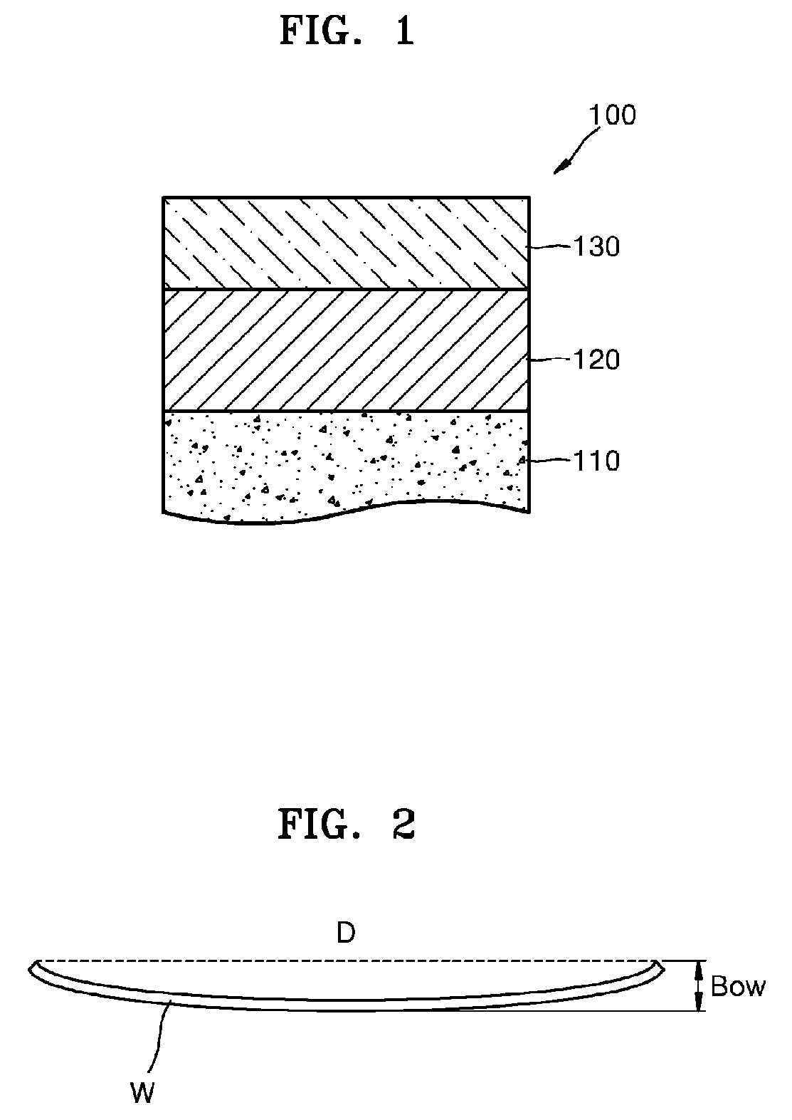
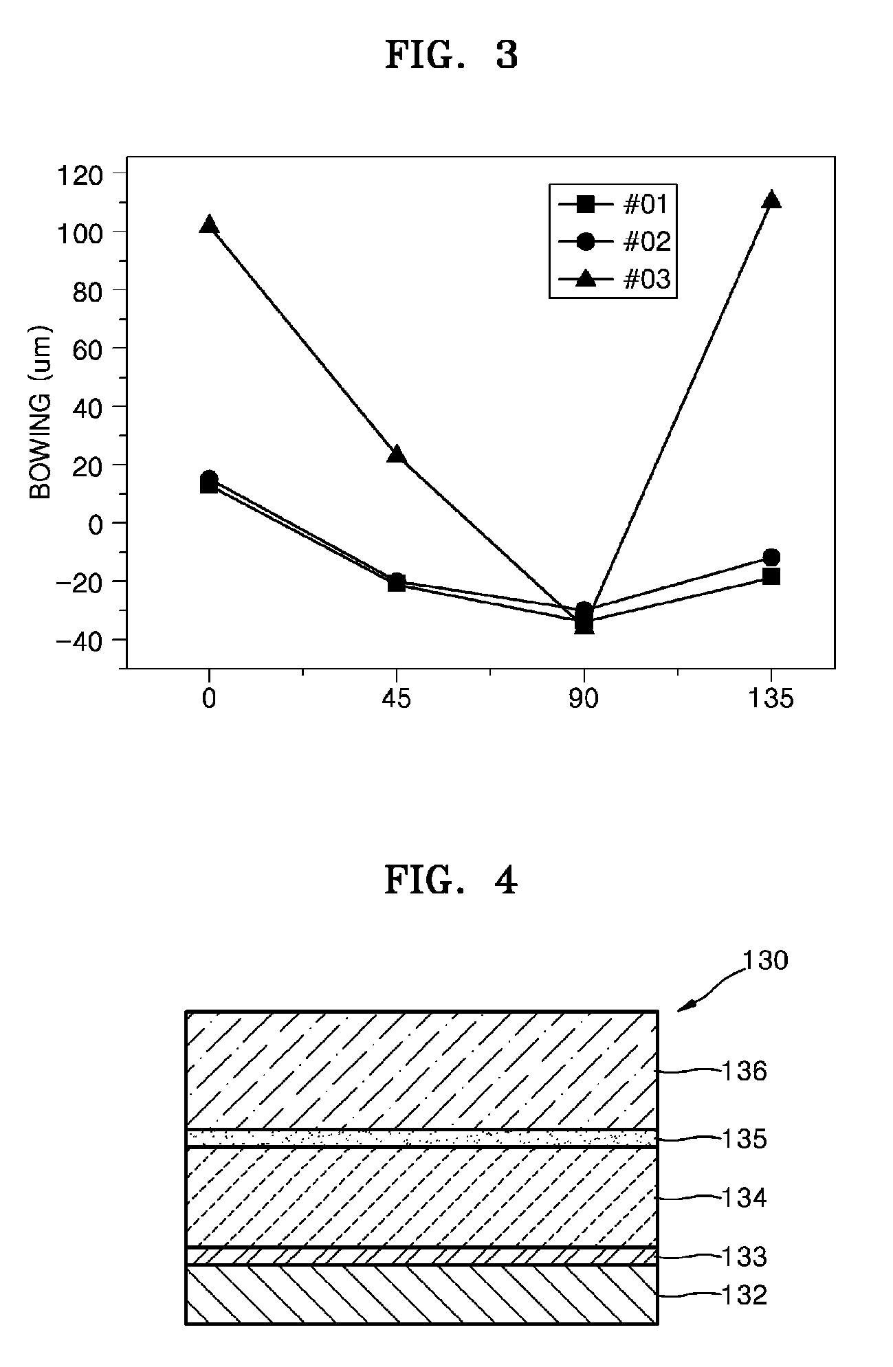
[0027]Example embodiments will now be described more fully with reference to the accompanying drawings, in which example embodiments are shown. The same reference numerals in the drawings denote the same elements, and sizes or thicknesses of elements may be exaggerated for clarity. Example embodiments are described herein and various modifications may be made in the embodiments. When a layer is referred to as being “on” or “over” another layer or a substrate, it may be directly on the other layer or the substrate, or intervening layers may also be present therebetween. As used herein, the term “and / or” includes any and all combinations of one or more of the associated listed items. Expressions such as “at least one of,” when preceding a list of elements, modify the entire list of elements and do not modify the individual elements of the list.

[0028]It will be understood that, although the terms “first”, “second”, etc. may be used herein to describe various elements, components, regio...


PUM

PropertyMeasurementUnit
resistivityaaaaaaaaaa
slip lengthaaaaaaaaaa

Abstract

A gallium nitride based semiconductor device includes a silicon-based layer doped simultaneously with boron (B) and germanium (Ge) at a relatively high concentration, a buffer layer on the silicon-based layer, and a nitride stack on the buffer layer. A doping concentration of boron (B) and germanium (Ge) may be higher than 1×10¹⁹ / cm3.

Description

CROSS-REFERENCE TO RELATED APPLICATION[0001]This application claims the benefit of Korean Patent Application No. 10-2012-0062862, filed on Jun. 12, 2012, in the Korean Intellectual Property Office, the disclosure of which is incorporated herein in its entirety by reference.BACKGROUND[0002]1. Field[0003]Example embodiments relate to gallium nitride based (AlxInyGa1−x−yN, 0≦x+y<1) semiconductor devices and methods of manufacturing the same, and more particularly, to gallium nitride based semiconductor devices that simultaneously reduce damage and deformation of a wafer and enhance uniformity of wavelengths of emitted light by reducing a bow of the wafer, and methods of manufacturing the same.[0004]2. Description of the Related Art[0005]GaN materials may be used together with AlN and InN to generate light having relatively wide bands from ultraviolet rays to red spectrum regions, and have relatively high dielectric breakdown characteristics. Thus, GaN materials are widely used to ma...

Claims


Application Information

Patent Timeline
Patent Type & Authority Patents(United States)
IPC IPC(8): H01L29/15H01L33/12H01L29/16H01L21/02H01L29/20H01L29/267H01L31/0256H01L33/00
CPCH01L29/267H01L21/0254H01L21/02381H01L21/02447H01L21/02488H01L29/16H01L29/2003H01L33/12H01L21/02458H01L33/007H01L33/32
Inventor TAK, YOUNG-JOKIM, JAE-KYUNKIM, JUN-YOUNLEE, JAE-WONCHOI, HYO-JI
Owner SAMSUNG ELECTRONICS CO LTD
Why Eureka
Try Eureka