Handle for semiconductor-on-diamond wafers and method of manufacture

a technology of diamond wafers and handle plates, which is applied in the direction of semiconductor/solid-state device details, thin material processing, semiconductor devices, etc., can solve the problems of reducing cooling requirements, gan and related ternary compounds exhibit relatively low thermal conductivity of the substrate commonly used, and the deficiency is the most pronounced, so as to reduce the bow of the sod wafers

Active Publication Date: 2018-01-30
AKASH SYST INC
View PDF25 Cites 2 Cited by
  • Summary
  • Abstract
  • Description
  • Claims
  • Application Information

AI Technical Summary

Benefits of technology

[0025]The carrier plate preferably has a low coefficient of linear thermal expansion so as to match the thermal characteristics of the semiconductor-on-diamond wafer. For example, the carrier plate may comprise a material having a coefficient of linear thermal expansion a at 20° C. in at least one plane of no more than: 10.0×10⁻⁶ K−1; 8.0×10⁻⁶ K−1; 6.0×10⁻⁶ K−1; 4.0×10⁻⁶ K−1; or 2.0×10⁻⁶ K−1. Ideally the material is a diamond material. For example, the carrier plate may be formed of a CVD diamond wafer or possible a diamond composite material such as silicon cemented diamond (ScD). It has been found that because the carrier plate and the semiconductor-on-diamond wafer need to be well matched over a wide range of physical and chemical conditions during device fabrication then a diamond carrier plate is advantageous. Furthermore, a diamond carrier plate can be re-used multiple times and is thus more commercially viable than other options.
[0034]It has also been found to be advantageous to provide a beveled edge to the adhesive layer in order to improve device fabrication steps. Further still, it has also been found to be advantageous to provide sealant over the adhesive by sealing areas on the composite wafer where adhesive is exposed with a high-temperature sealant and curing the high-temperature sealant.
[0037]The advantages of attaching the thin semiconductor-on-diamond wafer to a handle wafer is that handling thicker wafers is practical both manually and robotically / automatic. Second, CVD-grown diamond wafers include internal stresses and are generally bowed several times the common limit for wafer bow in commercial lithography tools. Attaching thin and bowed semiconductor-on-diamond wafers to thicker and flat diamond handle wafers significantly reduces the bow of the SOD wafers and makes them acceptable to industrial processing plants. DH surfaces are polished and the wafers can be held down by vacuum during lithography processing. Finally, thru via holes do not have to pass through to the DH wafer and hence have no influence on holding the composite wafers down with vacuum.

Problems solved by technology

In spite of the high-temperature performance, GaN and related ternary compounds exhibit relatively low thermal conductivity of the substrates commonly used for growth of GaN.
This deficiency is most pronounced in high-power microwave and millimeter-wave transistors and amplifiers where reduced cooling requirements and longer device life, both benefiting from lower junction temperature, are in critical demand.
Shortening the distance heat has to flow from the heat source to the highly thermally conductive heat spreaders and heatsink lowers the overall thermal resistance.
There is however one essential difference between working with diamond substrates and other common semiconductor substrates, such as, Gas, InP, and Silicon: diamond is hard to thin and polish (diamond grit is commonly used for thinning of other semiconductors), but most importantly, diamond wafer price increases with its thickness and hence it is difficult to justify using a diamond substrate thicker than is necessary both for thermal management purposes or chip handling purposes.
Since chip thicknesses and hence semiconductor-on-diamond wafers may range from tens of micrometers to several hundred micrometers, they are too thin for commercial foundry processing.
First, handling such thin wafers with diameters larger 25 mm is exceedingly difficult and not practical in neither manual nor robotic / automated processing.
Second, CVD-grown diamond wafers include internal stresses and exhibit bow that is several times larger than the common limit for wafer bow in commercial lithography tools.
Industrial processing plants will generally not accept wafers with such attributes.
Additionally, the diamond surface of the semiconductor-on-diamond wafer is often rough with average absolute roughness of several tens of micrometers which makes it more difficult to hold wafers down to a chuck using vacuum—a feature important in lithography processing.
Similar problems appear when thru-vias are used on wafers.

Method used


Image

  • Handle for semiconductor-on-diamond wafers and method of manufacture
  • Handle for semiconductor-on-diamond wafers and method of manufacture
  • Handle for semiconductor-on-diamond wafers and method of manufacture

Examples


Embodiment Construction

[0045]The specifications on the mechanical rigidity, flatness, chemical inertness and processing temperature of wafers manufactured in commercial foundries depend on the type of lithography, the specific manufacturer's recipes for contact anneal and chemical processing. Hence there are both mechanical, temperature processing, and chemical inertness constrains on the SOD and DH wafers. The target specifications addressed in this application are given as follows (they do not represent a limitation on the invention is used):

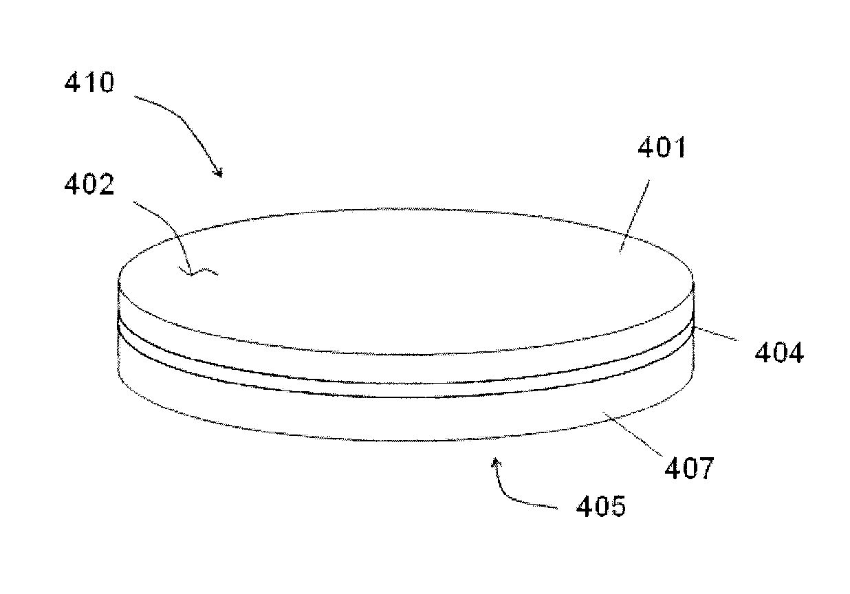
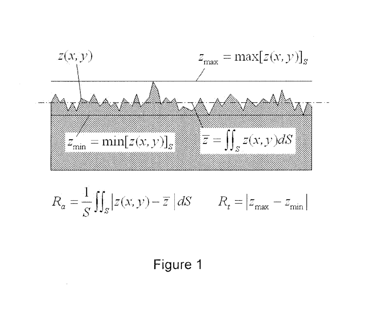
[0046]Starting GaN / Diamond wafer parameters are, but are not limited to the following:[0047]Average GaN / Diamond wafer thickness (WG): between 25 and 200 μm, typically 100 μm;[0048]Wafer diameter (DG): any standard wafer diameter;[0049]Maximum height of the surface profile (RtG): typical values are several tens of micrometers.

[0050]Starting diamond-carrier wafer parameters are, but are not limited to the following:[0051]Average diamond carrier-wafer thickness (Wc): t...


PUM


Abstract

Methods for mounting and dismounting thin and / or bowed semiconductor-on-diamond wafers (401) to a carrier (407) are disclosed that flatten said wafers and provide mechanical support to enable efficient semiconductor device processing on said semiconductor-on-diamond wafers.

Description

FIELD OF THE INVENTION[0001]The present invention relates to manufacturing of high-power electronic and optoelectronic devices on diamond wafers, and particularly relates to methods for providing a handle wafer as support for thin semiconductor-on-diamond wafers (<200 μm thick) so they can be efficiently handled in standard semiconductor-device manufacturing lines, and more particularly with gallium nitride on diamond wafers that are typically 100 μm thick to be processed in a standard semiconductor manufacturing line into high-electron mobility transistors, radio-frequency (RF) electronic devices, light-emitting-diodes, and lasers.BACKGROUND OF THE INVENTION[0002]Thermal management in semiconductor devices and circuits is a critical design element in any manufacturable and cost-effective electronic and optoelectronic product, such as light generation and electrical signal amplification. The goal of efficient thermal design is to lower the operating temperature of such electronic...

Claims


Application Information

Patent Timeline
Patent Type & Authority Patents(United States)
IPC IPC(8): H01L23/00H01L21/683H01L21/20H01L21/02H01L29/16H01L23/373H01L29/165
CPCH01L29/1602H01L21/02002H01L21/2007H01L21/6835H01L23/3732H01L24/29H01L24/98H01L29/165Y10T428/24355H01L2221/6835H01L2221/68318H01L2221/68381H01L2924/0002H01L2924/00011H01L21/0262
Inventor DIDUCK, QUENTINFRANCIS, DANIELLOWE, FRANK YANTISEJECKHAM, FELIX
Owner AKASH SYST INC
Why Eureka
Try Eureka