

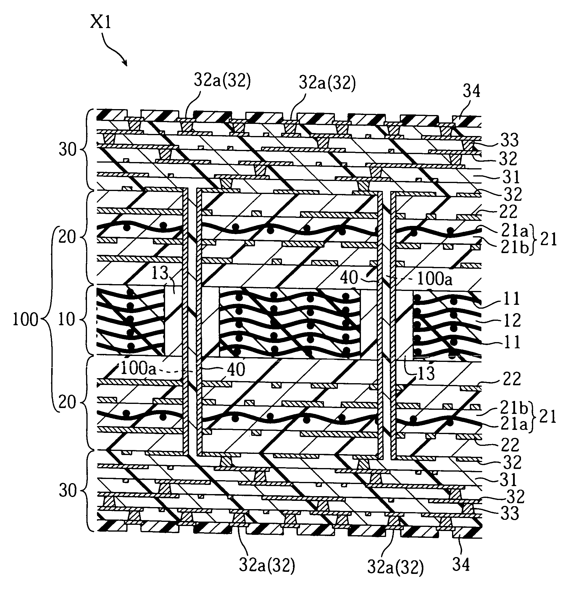
Multilayer wiring board, method for producing the same, and method for producing fiber reinforced resin board
a wiring board and multi-layer technology, applied in the direction of printed element electric connection formation, application, remote-control toys, etc., can solve the problems of low reliability of electrical connection between the wiring board and the semiconductor chip, easy cracking or peeling, and inability to secure sufficient connection reliability, etc., to achieve low elastic modulus, low elasticity, and low elasticity
- Summary
- Abstract
- Description
- Claims
- Application Information
AI Technical Summary
Benefits of technology
Problems solved by technology
Method used
Image

Examples
example 1
Creating a Multilayer Wiring Board
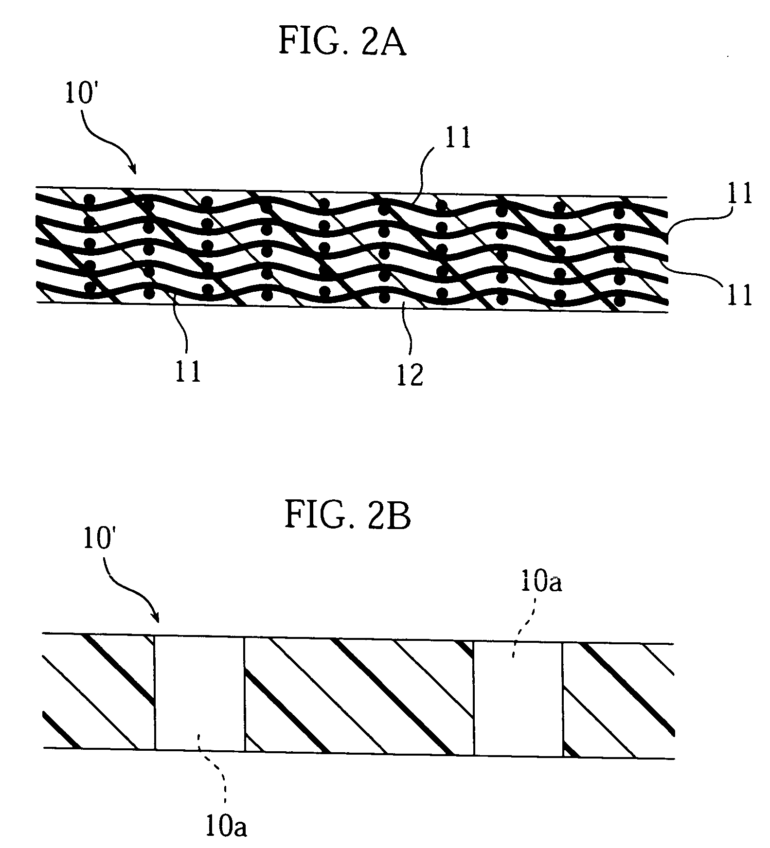
[0106] In this example, a compound of a carbon fiber cloth with an epoxy resin was used as a CFRP material. In creating a CFRP plate for this example, first of all, the carbon fiber cloth (Trade name: TORAYCA, produced by Toray Industries, Inc.) was impregnated with epoxy resin varnish (varnish which contains monomer or the like that is polymerized into epoxy resin), which is thereafter dried, and a prepreg with a thickness of 0.2 mm is created. This carbon fiber cloth is a plain fabric woven out of carbon fiber yarn which is obtained by bundling together an average of at least 1000 carbon fibers each of which has a cross-sectional diameter of 10 μm or less. Five of the prepreg prepared in the above manner were laminated and pressed in the lamination direction by a vacuum press for 30 minutes at a peak temperature of 200° C., thereby creating an unprocessed CFRP plate having a thickness of approximately 1.0 mm. The pressure to be applied at this mo...
example 2
Creating a Multilayer Wiring Board
[0119] In this example, a compound of a carbon fiber cloth and epoxy resin was used as a CFRP material. In creating a CFRP plate for this example, first of all, the carbon fiber cloth (Trade name: TORAYCA, produced by Toray Industries, Inc.) was impregnated with epoxy resin varnish (varnish which contains monomer or the like that is polymerized into epoxy resin), which is thereafter dried, and a prepreg with a thickness of 0.2 mm is created. This carbon fiber cloth is same as that of Example 1. Three of the prepreg prepared in the above manner were laminated and pressed in the lamination direction by a vacuum press for 30 minutes at a peak temperature of 200° C., thereby creating an unprocessed CFRP plate having a thickness of approximately 0.6 mm. The pressure to be applied at this moment was set to 40 kgf / cm2. The average coefficient of thermal expansion between 25° C. and 150° C. in the spread direction of the surface of the CFRP plate was 0.5 p...
PUM
| Property | Measurement | Unit |
|---|---|---|
| elastic modulus | aaaaa | aaaaa |
| Young's modulus | aaaaa | aaaaa |
| temperatures | aaaaa | aaaaa |
Abstract
Description
Claims
Application Information