Method for fabricating semiconductor device

a semiconductor wafer and semiconductor technology, applied in the field of semiconductor devices, can solve the problems of reducing the element yield, reducing the performance of the required element, and bowing of the sic substrate having a sic film formed by epitaxial growth, etc., and achieves the effect of reducing the bowing (deformation) of the semiconductor wafer, shape, and reducing the defect siz

Active Publication Date: 2010-05-18
LAPIS SEMICON CO LTD
View PDF2 Cites 2 Cited by
  • Summary
  • Abstract
  • Description
  • Claims
  • Application Information

AI Technical Summary

Benefits of technology

[0009]The present invention has been made in view of the circumstances as described above. The principal objects of the present invention are to provide the structure of a semiconductor device capable of reducing a bowing of a wafer, and a method for fabricating the semiconductor device.
[0010]Other objects of the present invention are to provide the structure of a semiconductor device capable of maintaining an element-forming region with high quality even after a SiC element forming process, and to provide a method for fabricating the semiconductor device.
[0019]The crystal-defect concentrated region can be intentionally formed by a predetermined method. In a SiC single crystal, adjustment of a growth plane can concentrate crystal defects such as dislocation and the like. These crystal defects can be concentrated further during growth of a film. On this account, a region other than a crystal-defect concentrated region becomes a high quality region in which crystal defects such as dislocation and the like are few.
[0020]In accordance with the present invention with the structure as described above, stresses of the silicon carbide (SiC) film on a semiconductor wafer can be relieved to reduce a bowing (deformation) of the semiconductor wafer. Also, a shape of the wafer bowing is discriminated in advance by a simulation in addition to an actual measurement. In accordance with the shape, an optimal groove shape and direction can be determined.
[0021]Alternatively, the grooves are made around the crystal-defect concentrated region in the silicon carbide (SiC) film, and therefore the crystal-defect concentrated region is separated spatially from a high quality region with few defects, by the grooves. Also, the grooves are made in the SiC film such that the crystal-defect concentrated region in the SiC film is removed. As a result, it is possible to restrain the crystal defect expansion (propagation) that the crystal-defect concentrated region in the SiC film effects during recrystallization of the SiC film, even if thermal treatment such as dopant activation or the like is performed at a high temperature.

Problems solved by technology

Although a SiC epitaxial film can be formed by various methods, defects have not been reduced sufficiently for the required element performance.
Recrystallization can spread a defect into a high quality region with few defects and furthermore can reduce the element yield.
Also, a large-diameter semiconductor wafer (with a diameter of, for example, 6 inches) is currently required, and therefore a bowing of a SiC substrate having a SiC film formed by epitaxial growth becomes a serious problem.
The SiC substrate with a large bowing equal to or more than several tens of μm (micrometer) makes a fine pattern formation difficult.

Method used


Image

  • Method for fabricating semiconductor device
  • Method for fabricating semiconductor device
  • Method for fabricating semiconductor device

Examples


Embodiment Construction

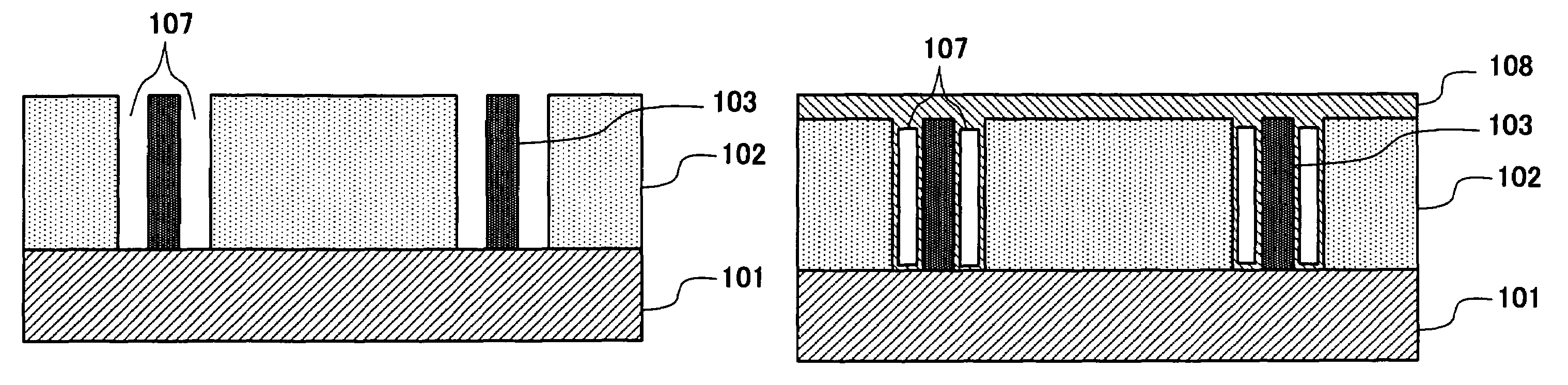
[0039]In the following detailed description of the preferred embodiments, reference is made to the accompanying drawings which form a part hereof, and in which is shown by way of illustration specific preferred embodiments in which the present invention may be practiced. These preferred embodiments are described in sufficient detail to enable those skilled in the art to practice the present invention, and it is to be understood that other preferred embodiments may be utilized and that logical, mechanical and electrical changes may be made without departing from the spirit and scope of the present invention. The following detailed description is, therefore, not to be taken in a limiting sense, and scope of the present invention is defined only by the appended claims.

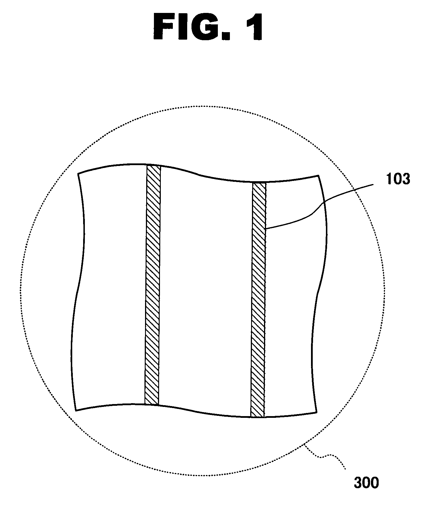
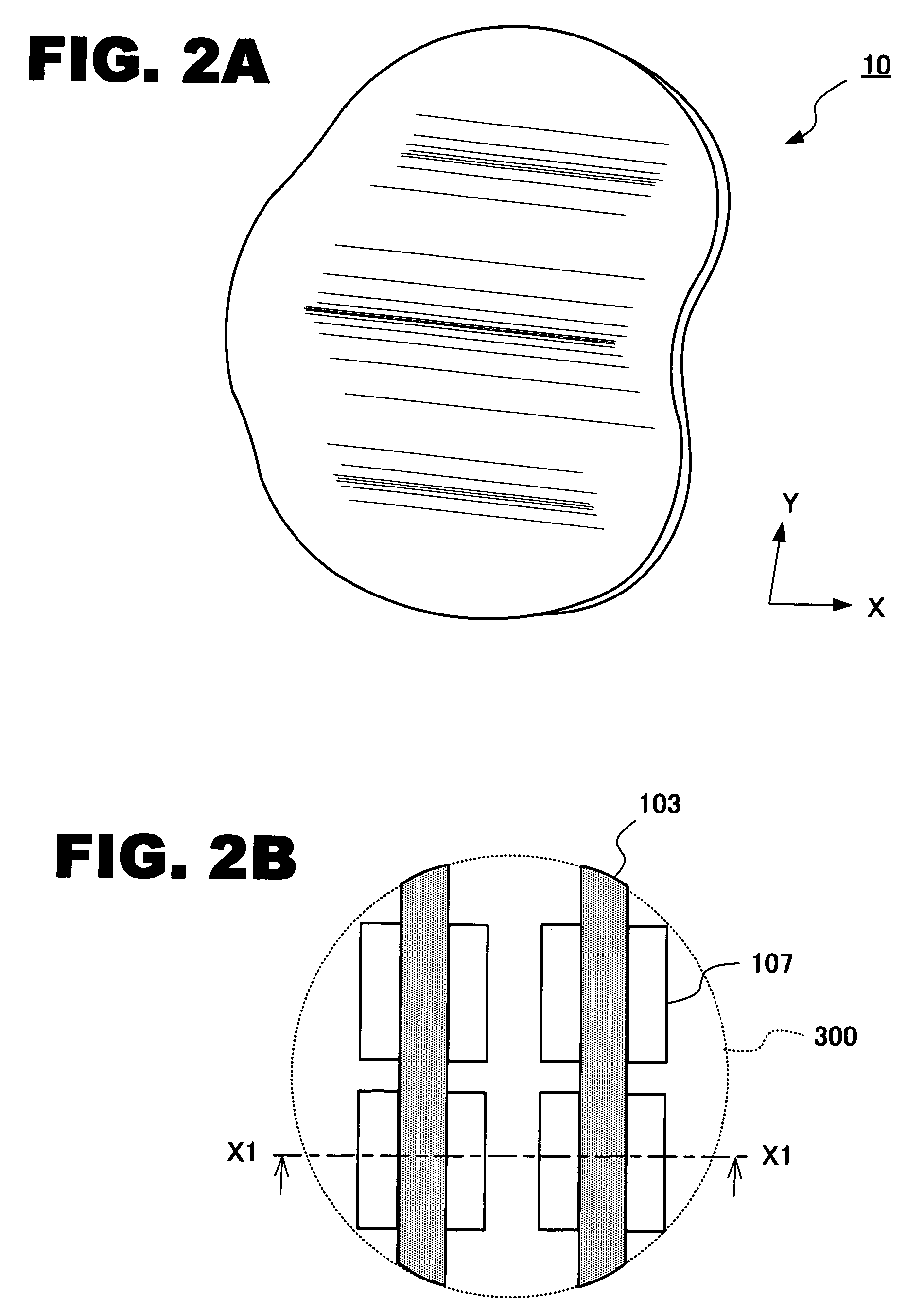
[0040]FIG. 1 is a schematic plan view showing, in part, structure of a semiconductor wafer 10 according to embodiments of the present invention.

[0041]In FIG. 1, reference numeral 103 indicates a crystal-defect concentrate...


PUM

PropertyMeasurementUnit
diameteraaaaaaaaaa
thicknessaaaaaaaaaa
thicknessaaaaaaaaaa

Abstract

The principal objects of the present invention are to provide structure of a semiconductor device capable of reducing a bowing of a wafer, and a method for fabricating the semiconductor device. The present invention is applied to a semiconductor device, which is fabricated with a semiconductor substrate having a silicon carbide (SiC) film. The method includes the steps of: forming the SiC film on a semiconductor wafer; discriminating a deformation condition of the semiconductor wafer; and forming grooves in the SiC film, the grooves having a shape determined in accordance with the deformation condition of the semiconductor wafer.

Description

CROSS REFERENCE TO RELATED APPLICATION[0001]This application claims the priority of Application No. 2007-071926, filed on Mar. 20, 2007 in Japan, the subject matter of which is incorporated herein by reference.TECHNICAL FIELD OF THE INVENTION[0002]This invention relates to a semiconductor device fabricated by using a semiconductor substrate having a silicon carbide (SiC) film, and a method for fabricating the semiconductor device.BACKGROUND OF THE INVENTION[0003]A power device using Si is employed in the field of power electronics such as motor control of a motor vehicle and an electric train, and the like. The insulation resistance of the power device depends on the performance limit of the power device. Therefore, there has been required the material having a wider band gap and higher breakdown field strength than Si. Silicon carbide (SiC), GaN, or diamond all has a wider band gap and higher breakdown field strength than Si. In addition, such material has the advantages such as a ...

Claims


Application Information

Patent Timeline
Patent Type & Authority Patents(United States)
IPC IPC(8): H01L21/20
CPCH01L21/046H01L21/0475H01L29/66712H01L21/3225H01L29/1608H01L29/66068
Inventor ABE, KAZUHIDE
Owner LAPIS SEMICON CO LTD
Why Eureka
Try Eureka