Defect inspection device using catadioptric objective lens
a technology of objective lens and defect inspection, which is applied in the direction of measuring device, optically investigating flaws/contamination, instruments, etc., can solve the problems of low s/n ratio, inability to achieve effective vertical illumination for detecting defects, and inability to free up the s/n ratio
- Summary
- Abstract
- Description
- Claims
- Application Information
AI Technical Summary
Problems solved by technology
Method used
Image

Examples
embodiment 1
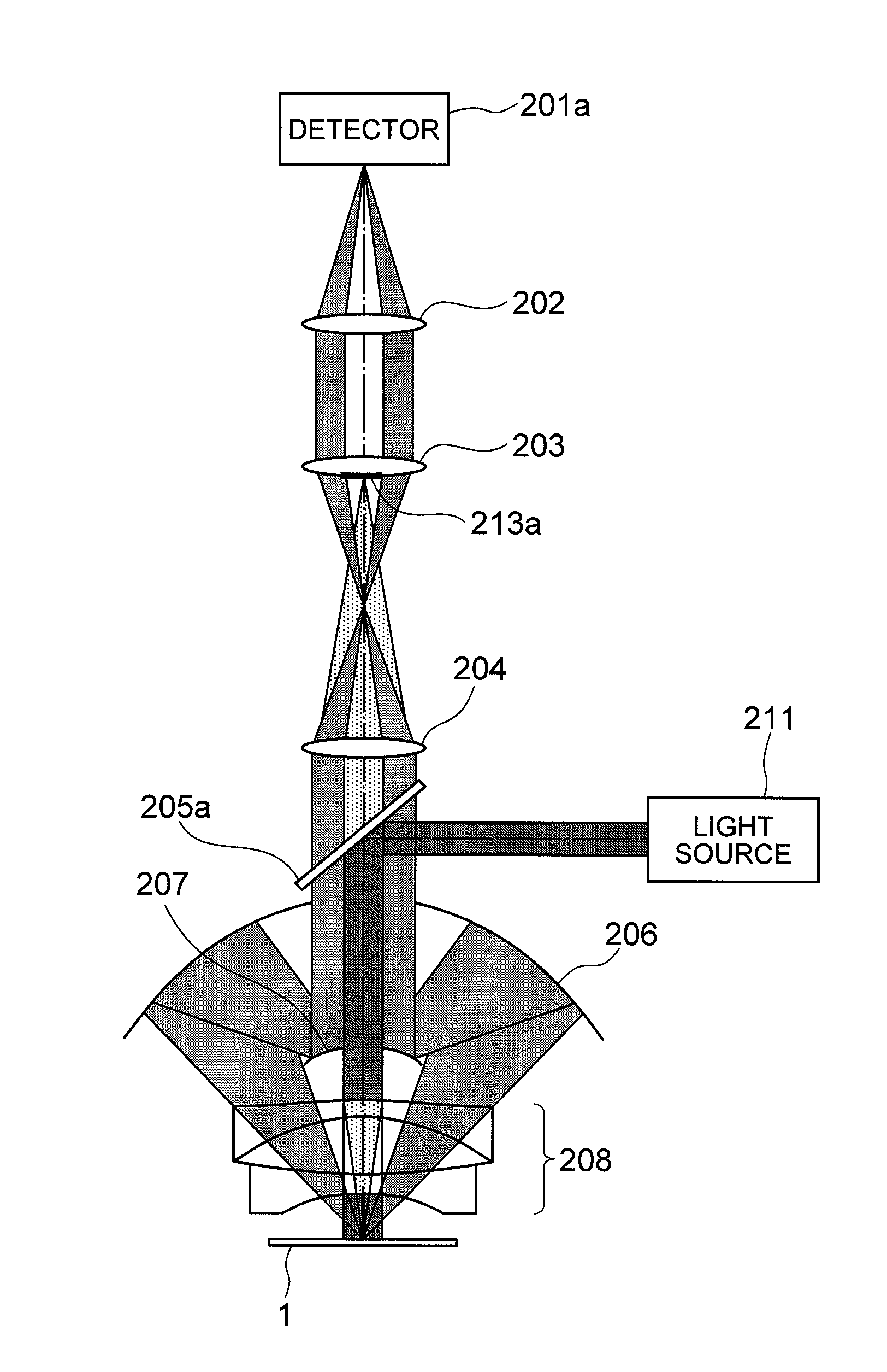
[0016]A first embodiment will be explained with reference to FIG. 1. FIG. 1 relates to an inspection optical system for inspecting a to-be-inspected object (wafer) 1.
[0017]The inspection optical system includes an illumination light source 211 for emitting illumination light to the wafer 1, a half mirror 205a for turning back the illumination light illuminated by the illumination light source 211 and emitting the illumination light to the wafer 1, a catadioptric objective lens having a convex reflecting member 207, a convex reflecting surface 206 and a dioptric objective lens group 208, an imaging lens 204 for focusing the reflected light from the wafer 1 transmitted through the catadioptric objective lens, a blocking member 213a arranged at a position at which the specularly reflected light from the wafer 1 contained in the reflected light is focused by the imaging lens 204, a first relay lens 203 having the blocking member 213a, a second relay lens 202 for transmitting specularly ...
embodiment 2
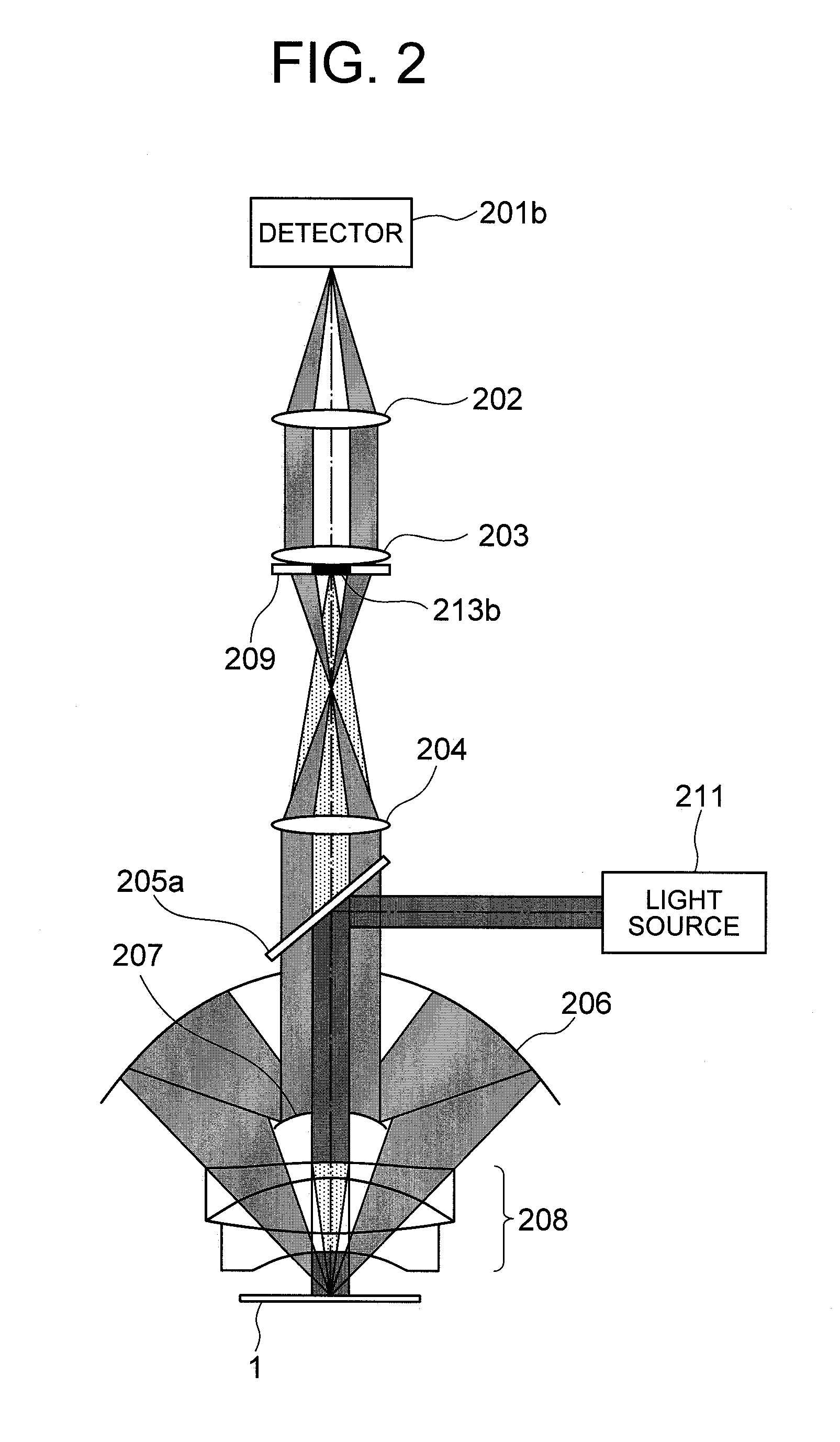
[0025]A second embodiment will be explained with referenced to FIG. 2. Here, only the difference from the first embodiment will be explained. The inspection optical system shown in FIG. 2 has the construction in which a spatial filter 209 having the blocking member 213b is arranged at a position at which the specularly reflected light from the wafer 1 is focused by the imaging lens 204. Because the specularly reflected light from the wafer 1 is blocked by the blocking member 213b provided to the spatial filter 209, the detector 201b detects only the scattered light from the wafer 1 and high S / N by the reduction of the flare component can be accomplished in the same way as in the first embodiment.
[0026]FIG. 9 shows an example of sectional and top views of a first relay lens 203, a spatial filter 209 and a blocking member 213b in the inspection optical system according to the second embodiment. However, the top view of the first relay lens 203 is shown deviated from that of the spatia...
embodiment 3
[0029]A third embodiment will be explained with referenced to FIG. 3. Here, only the differences from the first and second embodiments will be explained. In the inspection optical system shown in FIG. 3, a spatial filter 209 having a circular cylindrical turn-back mirror 213c is arranged at a position at which the specularly reflected light of the wafer 1 is focused and an illumination light source 211 is arranged in such a fashion that the rays of light can be turned back by this turn-back mirror 213c. This turn-back mirror 213c plays the role of the blocking member for blocking the specularly reflected light and the role of the turn-back member for turning back the illumination light and achieving vertical illumination.
[0030]FIG. 11 shows an example of sectional and top views of a first relay lens 203, a spatial filter 209 and a turn-back mirror 213c as a blocking member in the third embodiment. However, the top view of the first relay lens 203 is shown deviated from that of the s...
PUM
| Property | Measurement | Unit |
|---|---|---|
| wavelength | aaaaa | aaaaa |
| defect inspection | aaaaa | aaaaa |
| wavelengths | aaaaa | aaaaa |
Abstract
Description
Claims
Application Information
 - R&D
- Intellectual Property
- Life Sciences
- Materials
- Tech Scout
- Unparalleled Data Quality
- Higher Quality Content
- 60% Fewer Hallucinations
Browse by: Latest US Patents, China's latest patents, Technical Efficacy Thesaurus, Application Domain, Technology Topic, Popular Technical Reports.
© 2025 PatSnap. All rights reserved.Legal|Privacy policy|Modern Slavery Act Transparency Statement|Sitemap|About US| Contact US: help@patsnap.com