Electronic device housing and manufacturing method thereof

a technology for electronic devices and housings, applied in the direction of electric apparatus casings/cabinets/drawers, instruments, conductors, etc., can solve the problems of deteriorating device appearance and affecting appearan

Inactive Publication Date: 2013-12-10
FU TAI HUA IND SHENZHEN +1
View PDF2 Cites 3 Cited by
  • Summary
  • Abstract
  • Description
  • Claims
  • Application Information

AI Technical Summary

Benefits of technology

[0004]A typical electronic device housing includes a bottom housing, a side frame, and a display panel. The display panel is positioned on the side frame. A periphery of the side frame is welded to the bottom housing. However, after welding, a welding portion between the side frame and the bottom housing may generate weld marks, deteriorating the device's appearance. The side frame can also be fixed to the bottom housing via a plurality of screws. However, in assembly of the electronic device housing, the plurality of screws should be operated in turns and a gap may be generated between the side frame and the bottom housing, also affecting appearance.

Problems solved by technology

However, after welding, a welding portion between the side frame and the bottom housing may generate weld marks, deteriorating the device's appearance.
However, in assembly of the electronic device housing, the plurality of screws should be operated in turns and a gap may be generated between the side frame and the bottom housing, also affecting appearance.

Method used


Image

  • Electronic device housing and manufacturing method thereof
  • Electronic device housing and manufacturing method thereof
  • Electronic device housing and manufacturing method thereof

Examples


Embodiment Construction

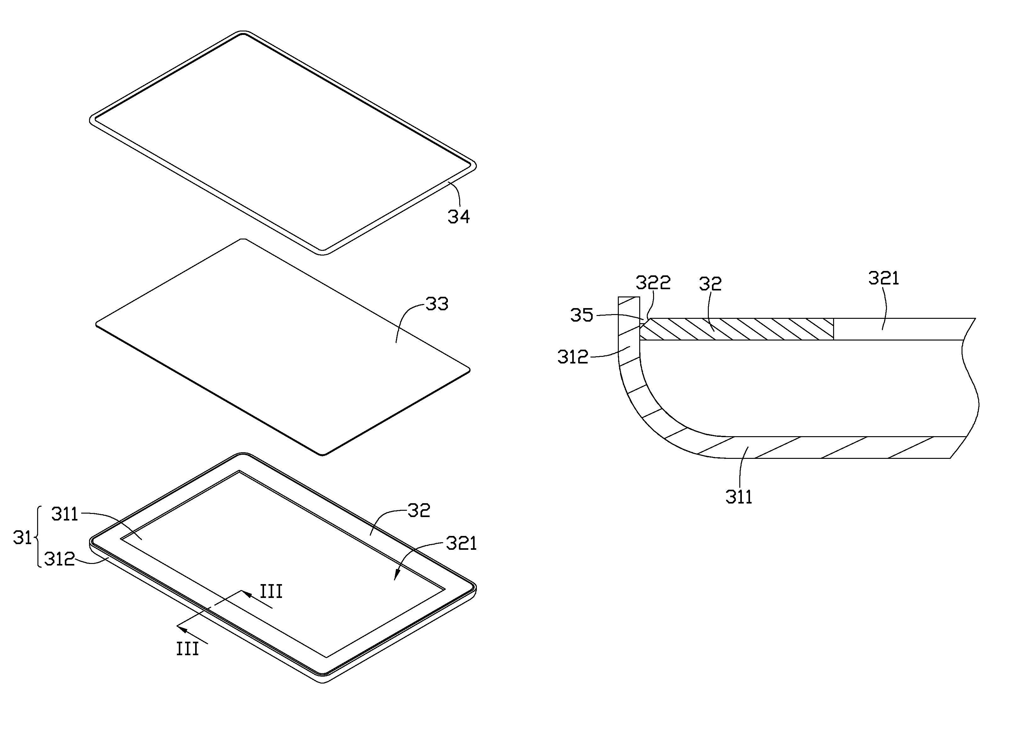
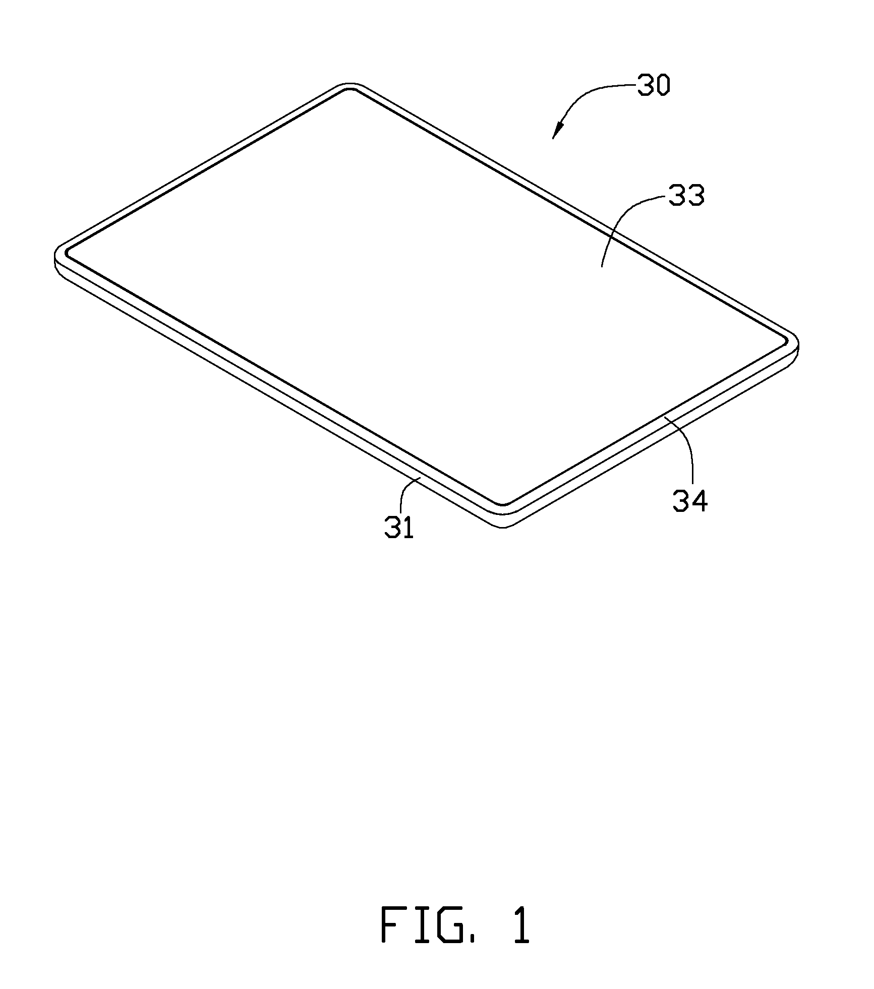
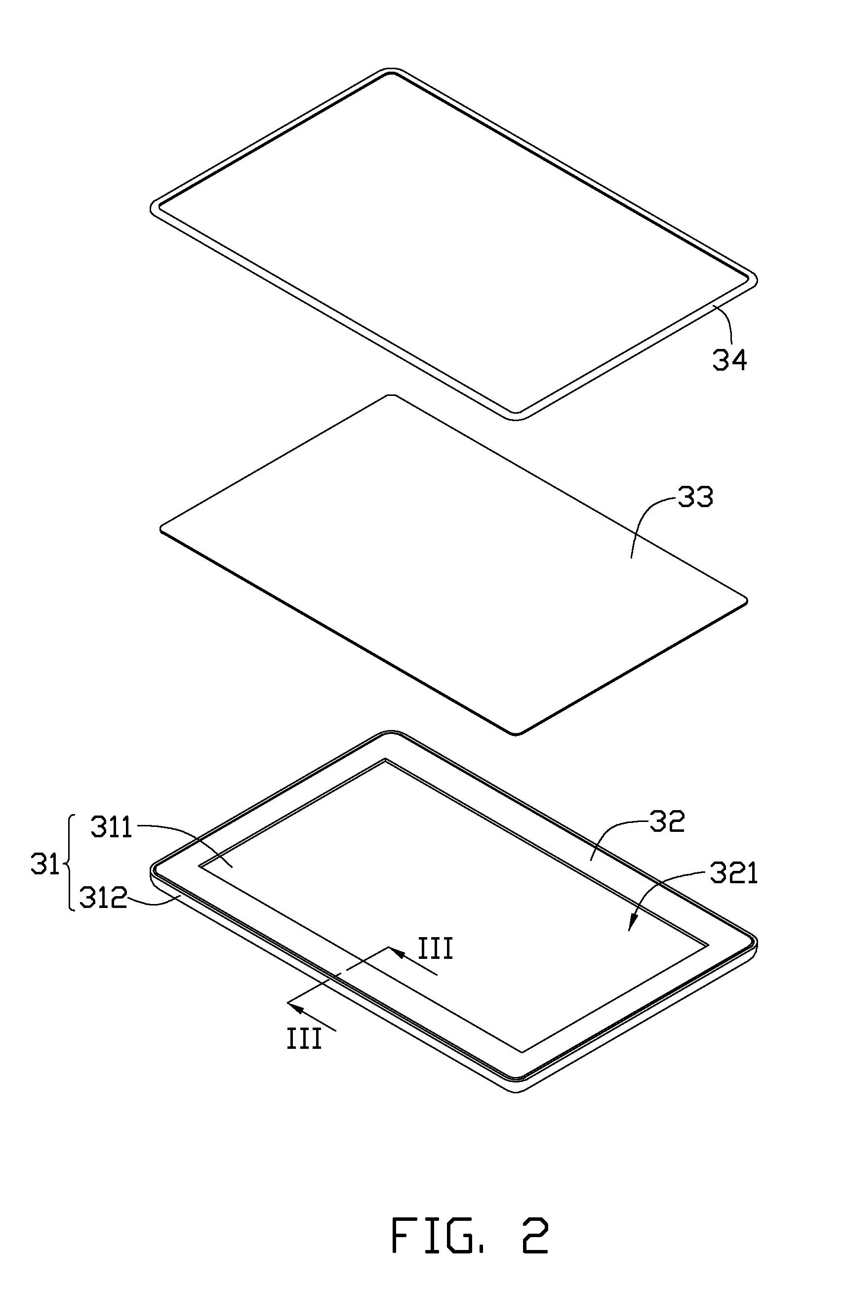
[0010]Referring to FIGS. 1 through 3, an embodiment of an electronic device housing 30 includes a bottom housing 31, a support plate 32, a display panel 33, and a side frame 34. The support plate 32 is welded in the bottom housing 31. The display panel 33 is positioned on the support plate 32. The side frame 34 is connected to a top edge of the bottom housing 31.

[0011]The bottom housing 31 includes a base plate 311 and a curved sidewall 312 extending from an edge of the base plate 311. In the illustrated embodiment, the bottom housing 31 is made of metal materials, such as aluminum.

[0012]The support plate 32 defines a through hole 321 in a center portion. The support plate 32 further forms an angled portion 322 (see FIG. 3) on an edge of the support plate 32 adjacent the sidewall 312. In the illustrated embodiment, the support plate 32 is substantially rectangular, and the through hole 321 is substantially rectangular. The support plate 32 is made of metal materials, such as aluminu...


PUM

PropertyMeasurementUnit
plasticaaaaaaaaaa
heightaaaaaaaaaa
external forceaaaaaaaaaa

Abstract

An electronic device housing includes a bottom housing, a support plate, a display panel, and a side frame. The support frame is welded in the bottom housing. The display panel is positioned on the support plate. The side frame is connected to a top edge of the bottom housing, such that the display panel is sandwiched between the support plate and the side frame. A manufacturing method for an electronic device housing is also provided.

Description

BACKGROUND[0001]1. Technical Field[0002]The present disclosure relates generally to electronic device housings, more particularly, to an electronic device housing manufactured by welding.[0003]2. Description of Related Art[0004]A typical electronic device housing includes a bottom housing, a side frame, and a display panel. The display panel is positioned on the side frame. A periphery of the side frame is welded to the bottom housing. However, after welding, a welding portion between the side frame and the bottom housing may generate weld marks, deteriorating the device's appearance. The side frame can also be fixed to the bottom housing via a plurality of screws. However, in assembly of the electronic device housing, the plurality of screws should be operated in turns and a gap may be generated between the side frame and the bottom housing, also affecting appearance.[0005]Therefore, there is room for improvement within the art.BRIEF DESCRIPTION OF THE DRAWINGS[0006]The components ...

Claims


Application Information

Patent Timeline
Patent Type & Authority Patents(United States)
IPC IPC(8): H05K5/00H04M1/00H05K7/00
CPCB23K26/243B23K26/3213B23P15/00B23K2201/04B23K2201/38B23K2203/10B23K26/32B23K26/242B23K2101/04B23K2101/38B23K2103/08B23K2103/10B23K2103/42
Inventor WANG, CONG-CONGTANG, ZI-MINGSHI, FA-GUANGYUAN, JING-HUA
Owner FU TAI HUA IND SHENZHEN
Why Eureka
Try Eureka