Lens assembly and electronic device including the same

a technology of electronic devices and lenses, applied in the field of optical devices, can solve the problems of compromising the performance of electronic devices, high-performance, and high-power consumption, and achieve the effects of limiting the design of devices, improving quality, and improving quality

Active Publication Date: 2021-05-06
SAMSUNG ELECTRONICS CO LTD
View PDF2 Cites 2 Cited by
  • Summary
  • Abstract
  • Description
  • Claims
  • Application Information

AI Technical Summary

Benefits of technology

[0005]According to an embodiment, as the opening area through which light is incident from the outside onto the lens assembly increases, the lens assembly may obtain images or video with better quality. However, the opening area is exposed to the outside of the electronic device, and a larger size of the opening area may deteriorate the appearance of the electronic device or may limit how the device can be designed. For example, a lens assembly with a larger opening area may obtain images with better quality but may cause the electronic device to look ugly.
[0006]According to another embodiment, an electronic device may include a lens assembly for user authentication (e.g., iris or face recognition), video calls, or selfie taking. The lens assembly may be, at least, partially exposed from the front surface of the electronic device, reducing the active area of the display relative to the whole area of the electronic device. For example, when the lens assembly is installed to be able to capture what is in front of the electronic device, the display size relative to the actual size of the electronic device, which the user may find to be more important, may be reduced.

Problems solved by technology

However, portability and appearance may compromise the performance of electronic device.
For example, high-performance, large-screen displays may output high-definition screens but suffer from poor portability.
As another example, as displays output larger screens with higher performance, the control circuitry may be more complicated or consume more power.
However, the opening area is exposed to the outside of the electronic device, and a larger size of the opening area may deteriorate the appearance of the electronic device or may limit how the device can be designed.
For example, a lens assembly with a larger opening area may obtain images with better quality but may cause the electronic device to look ugly.

Method used


Image

  • Lens assembly and electronic device including the same
  • Lens assembly and electronic device including the same
  • Lens assembly and electronic device including the same

Examples


Embodiment Construction

TION

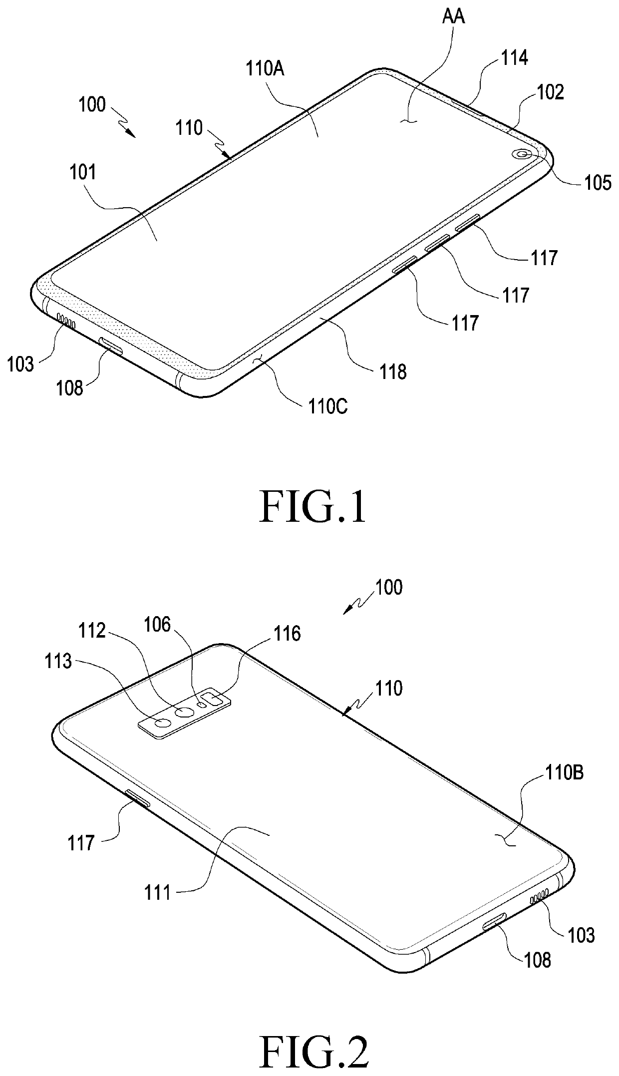
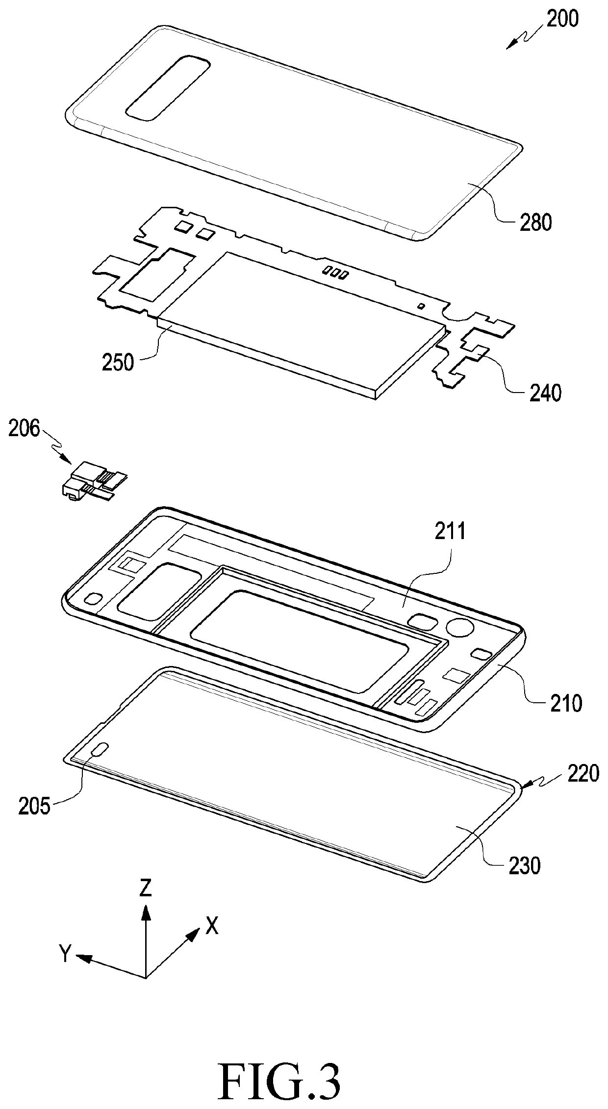
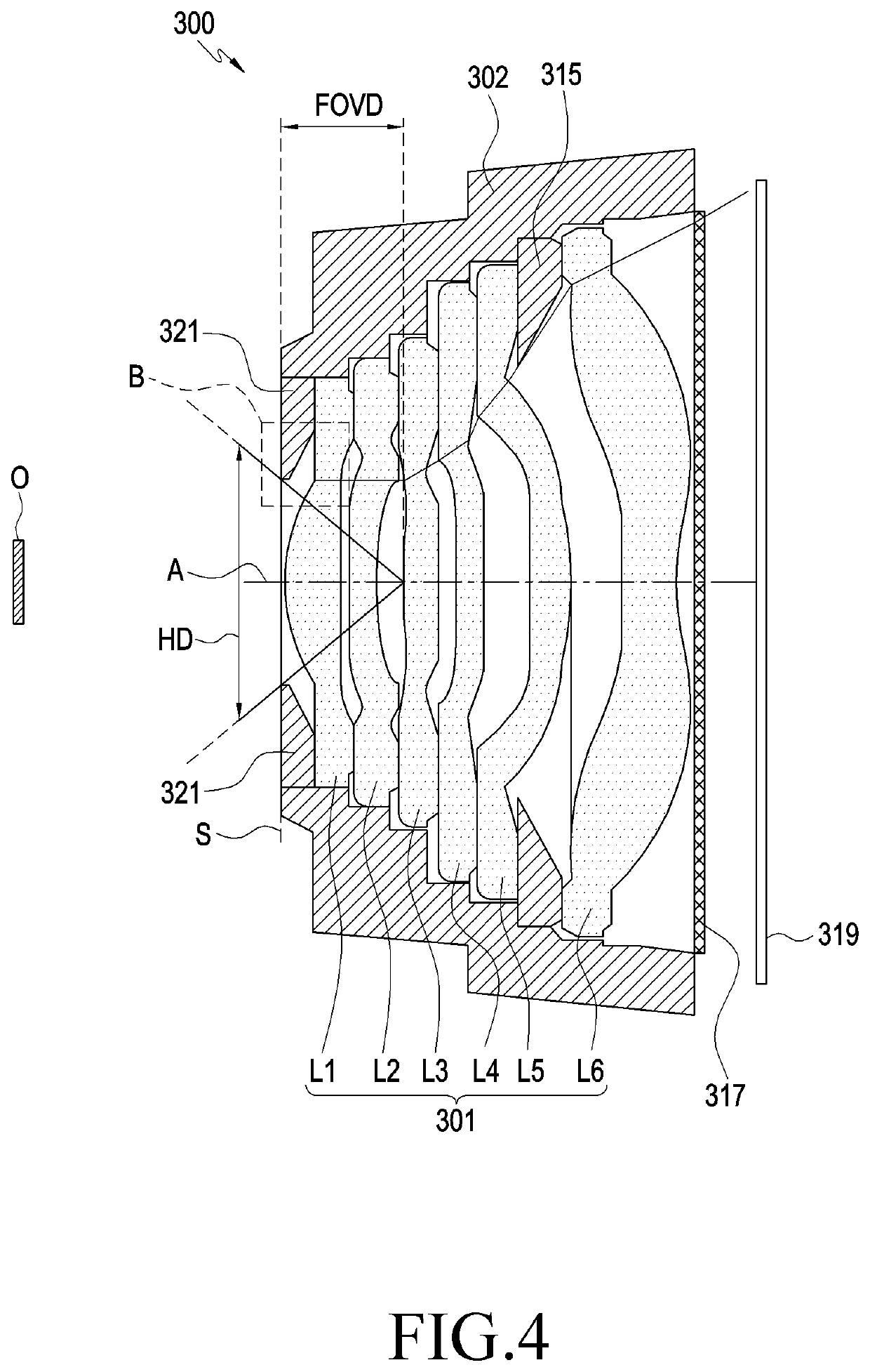
[0031]According to certain embodiments, there may be provided a lens assembly with a smaller opening area formed in a portion of the display to allow light to be incident from the outside of the electronic device to the image sensor inside the electronic device. An electronic device including the lens assembly is also provided.

[0032]According to certain embodiments, there may be provided a lens assembly with a miniaturized opening area. through which light is incident. The lens assembly is still capable of obtaining high-quality images. An electronic device including the lens assembly is also provided.

[0033]As the disclosure allows for various changes and numerous embodiments, various example embodiments will be described in greater detail with reference to the accompanying drawings. However, it should be understood that the disclosure is not limited to the specific embodiments, and that the disclosure includes all modifications, equivalents, and alternatives within the spirit a...


PUM


Abstract

Disclosed herein is a lens assembly that includes an aperture stop and at least three lenses. The first lens is disposed closer to the image sensor than the aperture stop, the first lens including two convex surfaces. The second lens is disposed closer to the image sensor than the first lens, and includes convex and concave surfaces. And the third lens is disposed closer to the image sensor than the second lens. The lens assembly meets Equation 1:0.1≤CT15 / StopL≤0.4wherein “CT15” denotes a distance between the object-side surface of the first lens and the object-side surface of the third lens measured along the optical axis, and “StopL” denotes a distance between an image forming surface of the image sensor and the aperture stop measured along the optical axis. Other various embodiments are also disclosed.

Description

CROSS-REFERENCE TO RELATED APPLICATION(S)[0001]This application is based on and claims priority under 35 U.S.C. 119 to Korean Patent Application No. 10-2019-0140826, filed on Nov. 6, 2019, in the Korean Intellectual Property Office, the disclosure of which is herein incorporated by reference in its entirety.BACKGROUNDField[0002]One or more embodiments of the instant disclosure generally relate to optical devices, e.g., lens assemblies and / or electronic devices including the lens assemblies.Description of Related Art[0003]Optical devices, for example, cameras capable of capturing images or videos have been widely used, and digital cameras or video recorders with digital image sensors such as a charge coupled device (CCD) or complementary metal-oxide semiconductor (CMOS) have become commonplace. As optical technology has gradually developed, image sensors or image sensor-equipped lens assemblies are being miniaturized and implemented in portable electronic devices, such as mobile comm...

Claims


Application Information

Patent Timeline
Patent Type & Authority Applications(United States)
IPC IPC(8): G02B13/00G02B5/00G02B9/62
CPCG02B13/0045G02B9/62G02B5/005G02B7/021G03B9/02G02B13/18G03B30/00
Inventor KIM, HYUNJEAKIM, CHANGKEUNKIM, HYUNHOBAE, JAECHEOLLEE, KYEONGEUN
Owner SAMSUNG ELECTRONICS CO LTD
Why Eureka
Try Eureka