Counting circuit of semiconductor device and duty correction circuit of semiconductor device using the same

a duty correction circuit and semiconductor technology, applied in the field of semiconductor devices, can solve the problems of short lock time, binary search method disadvantage, linear search method disadvantage, etc., and achieve the effect of minimizing the probability of an error occurring during an operation

Active Publication Date: 2014-01-07
SK HYNIX INC
View PDF3 Cites 0 Cited by
  • Summary
  • Abstract
  • Description
  • Claims
  • Application Information

AI Technical Summary

Benefits of technology

[0017]Due to this fact, it is possible to take only the advantages of the various methods for changing the values of counting codes until the values reach preset target values, and the probability of an error to occur during an operation may be minimized.

Problems solved by technology

In this way, the locking time is short since the values of the duty correction codes in the duty correction operation are changed by a substantial amount.
However, after the duty cycle of the input clock is corrected to 50% in the initial duty correction operation, the binary search method has a disadvantage because a substantial amount of change in the values of the duty cycle correction codes occurs even to detect a fine duty error.
More specifically, as shown in FIGS. 3 and 4, the linear search method has a disadvantage because the locking time is very long because the duty correction codes change by a small amount.
Nevertheless, a circuit implementing both the binary search method and the linear search method may have additional complexity.

Method used


Image

  • Counting circuit of semiconductor device and duty correction circuit of semiconductor device using the same
  • Counting circuit of semiconductor device and duty correction circuit of semiconductor device using the same
  • Counting circuit of semiconductor device and duty correction circuit of semiconductor device using the same

Examples


first embodiment

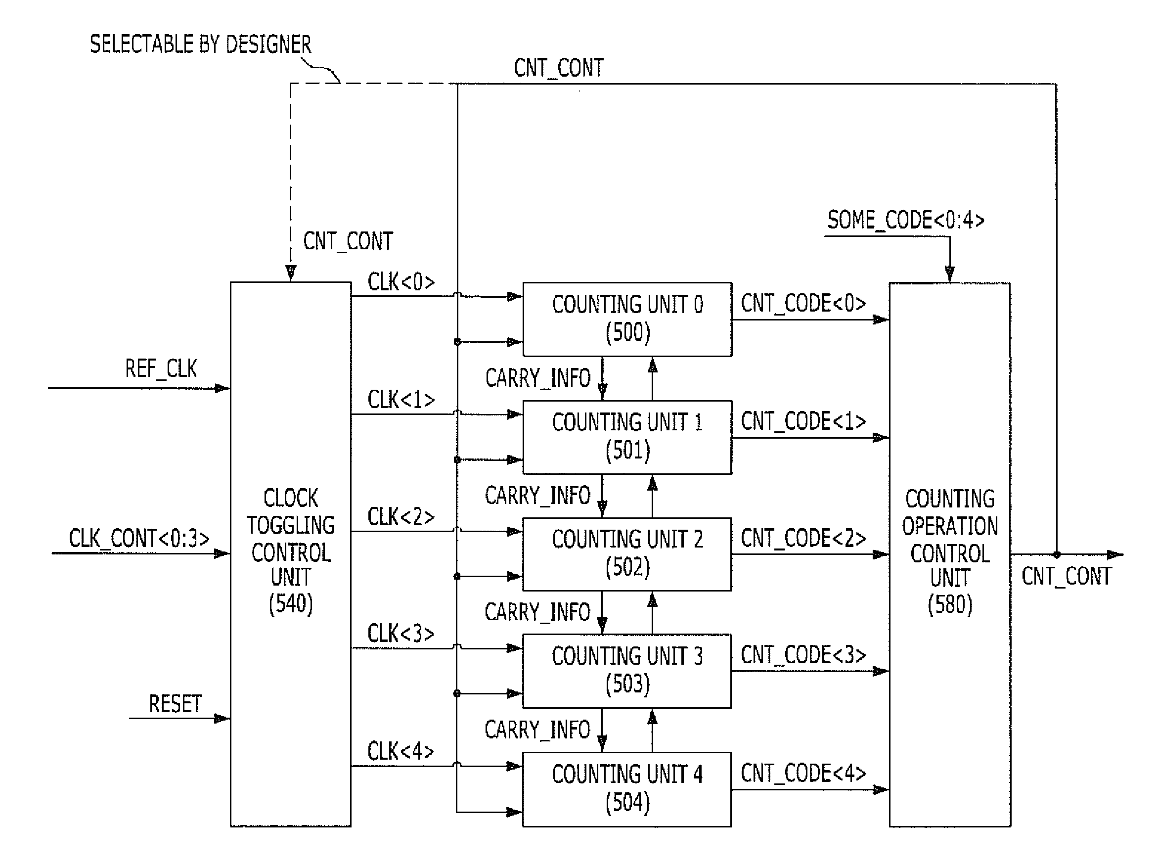
[0034]The detailed configuration of the clock toggling control unit 540 will be described below with reference to FIG. 6. The clock toggling control unit 540 includes a toggling operation control signal generation part 542 configured to generate a plurality of toggling operation control signals TOGGL_CONT. The clock toggling control unit 540 also includes a plurality of counting clock generation parts 544 configured to generate the counting clocks CLK in response to the respective toggling operation control signals TOGGL_CONT and the source clock REF_CLK. The toggling operation control signals TOGGL_CONT are sequentially activated from a deactivated signal each time the source clock REF_CLK toggles during the period when the counting control signal CNT_CONT is deactivated. Also, the toggling operation control signals TOGGL_CONT are all activated, or determined not to be active, during the period when the counting control signal CNT_CONT is activated in the initial operations of the...

second embodiment

[0043]The detailed configuration of the clock toggling control unit 540 will be described below with reference to FIG. 6. The clock toggling control unit 540 includes a toggling operation control signal generation part 542 configured to generate a plurality of toggling operation control signals TOGGL_CONT. The clock toggling control unit 540 also includes a plurality of counting clock generation parts 544 configured to generate the counting clocks CLK in response to the respective toggling operation control signals TOGGL_CONT and the source clock REF_CLK. The toggling operation control signals TOGGL_CONT are sequentially activated each time a source clock REF_CLK toggles. All of the toggling operation control signals TOGGL_CONT are activated, or determined not to be activated, when the number of activated signals is equal to or greater than the designated number.

[0044]The toggling operation control signal generation part 542 includes an initialization determining section 5422 and a...


PUM


Abstract

A counting circuit of a semiconductor device includes a plurality of counting units configured to count respective bits of counting codes in response to a plurality of counting clocks, respectively, and to control in a counting direction in response to a counting control signal; a clock toggling control unit configured to control the number of counting clocks that toggle among the plurality of counting clocks in response to clock control signals; and a counting operation control unit configured to compare a value of target codes and a value of the counting codes, and to determine a value of the counting control signal according to a comparison result.

Description

CROSS-REFERENCE TO RELATED APPLICATIONS[0001]The present application claims priority of Korean Patent Application No. 10-2011-0077463, filed on Aug. 3, 2011, which is incorporated herein by reference in its entirety.BACKGROUND[0002]1. Field[0003]Exemplary embodiments of the present invention relate to semiconductor devices, and more particularly, to a counting circuit of a semiconductor device and a duty correction circuit of a semiconductor device that are implemented to the counting circuit of a semiconductor device.[0004]2. Description of the Related Art[0005]The duty cycle of a clock is the ratio of the duration that an input clock is at a high logic level, or a low logic level, to the total period of the input clock signal. A circuit for detecting the duty cycle of an input clock generates a value indicating that the duty of a period is larger or smaller than 50%, and a duty correction circuit performs an operation to correct the duty cycle of the input clock by using the value...

Claims


Application Information

Patent Timeline
Patent Type & Authority Patents(United States)
IPC IPC(8): H03K21/00
CPCH03K21/38H03K5/1565G11C7/22
Inventor CHOI, HAE-RANGKIM, YONG-JU
Owner SK HYNIX INC
Why Eureka
Try Eureka