Spacer for a capacitive microphone and capacitive microphone with the same
a capacitive microphone and spacer technology, applied in the field of capacitive microphones, can solve the problems of deteriorating product sensibility limits, increasing fabrication difficulty and cost, and affecting product performance, so as to reduce product manufacturing costs, effectively prevent the effect of occurring, and improve the quality of products
- Summary
- Abstract
- Description
- Claims
- Application Information
AI Technical Summary
Benefits of technology
Problems solved by technology
Method used
Image
Examples
first embodiment
[0025]The spacer for a capacitive microphone according to the present invention will be described in detail with reference to drawings in below.
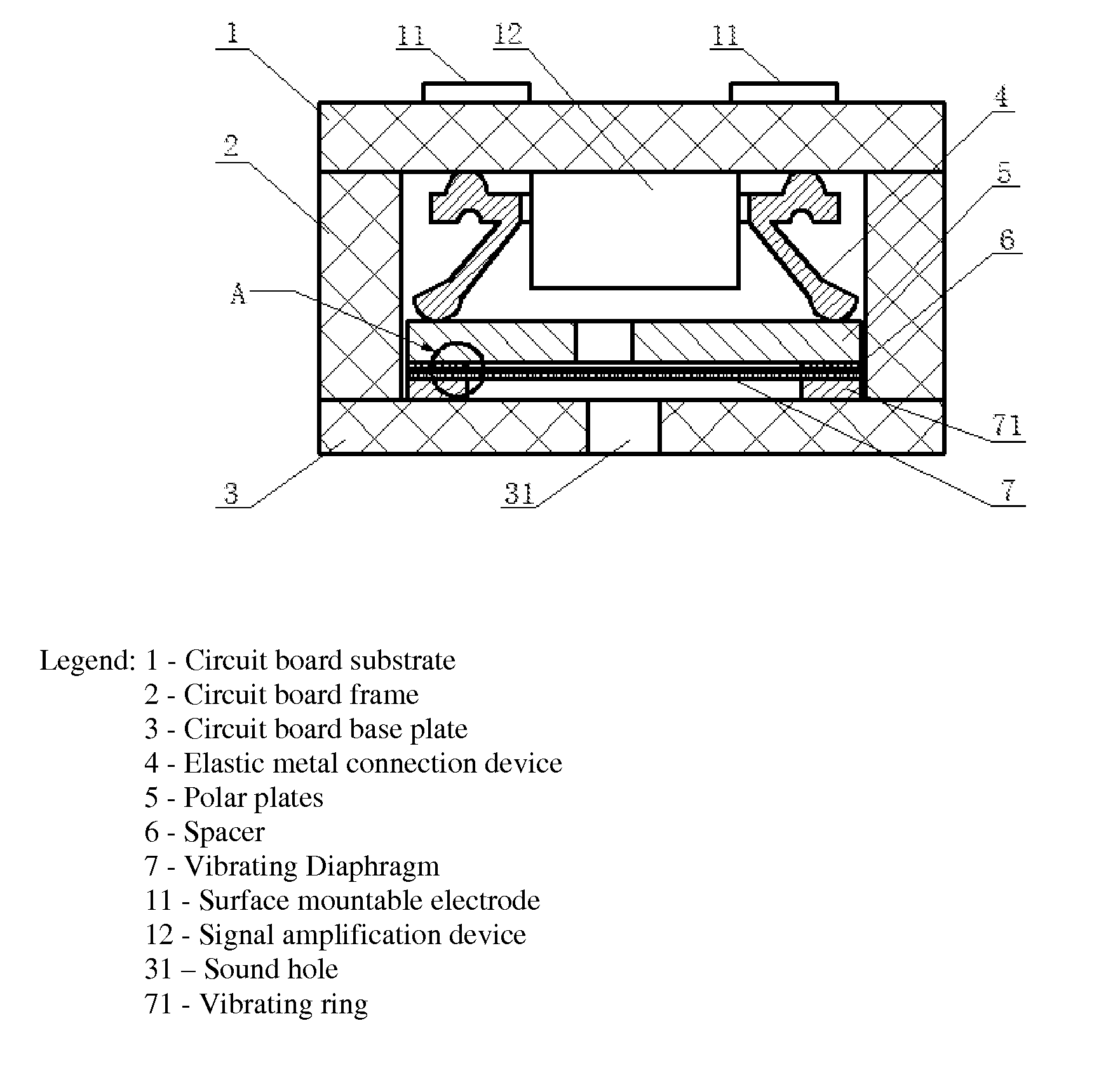
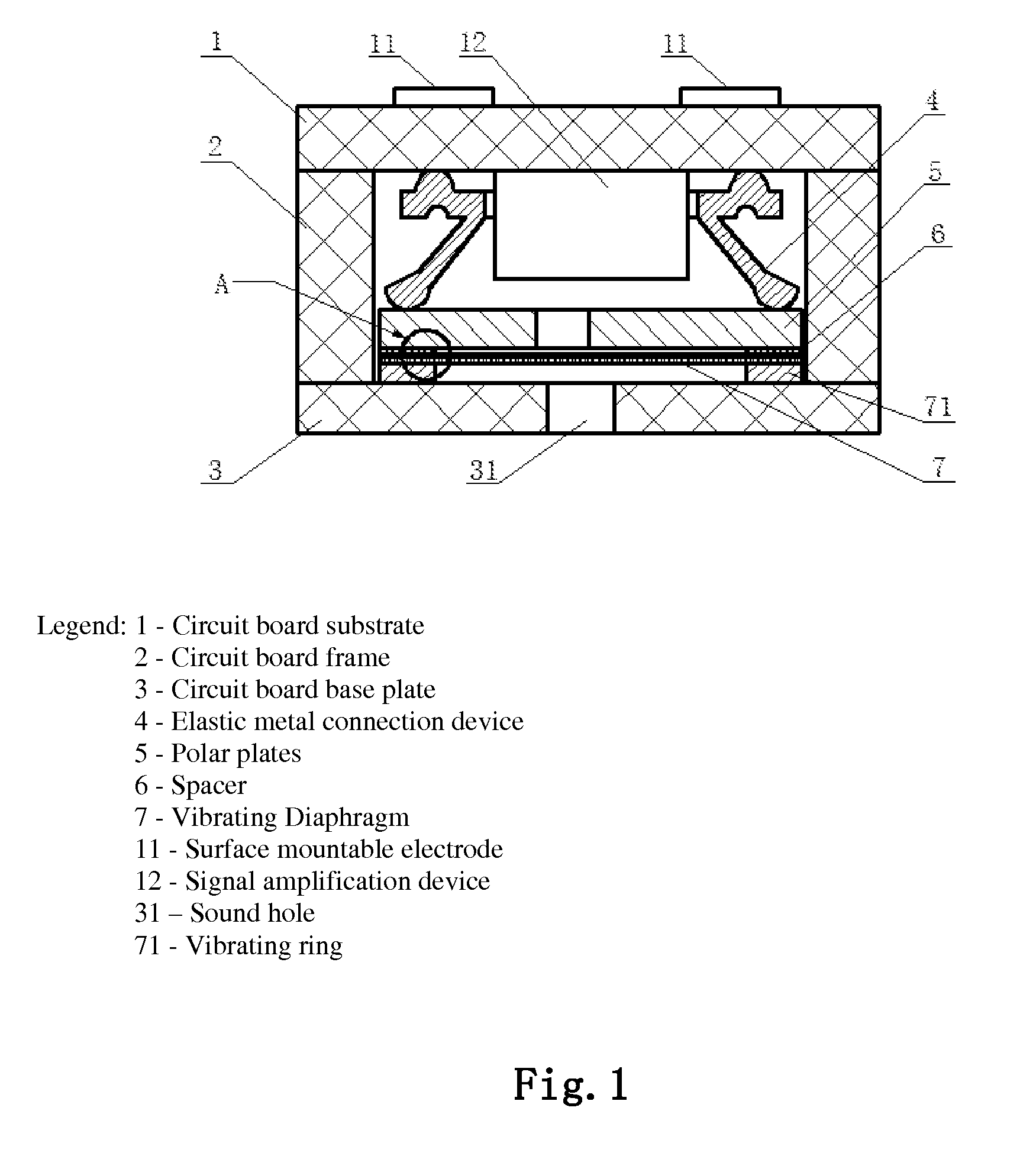
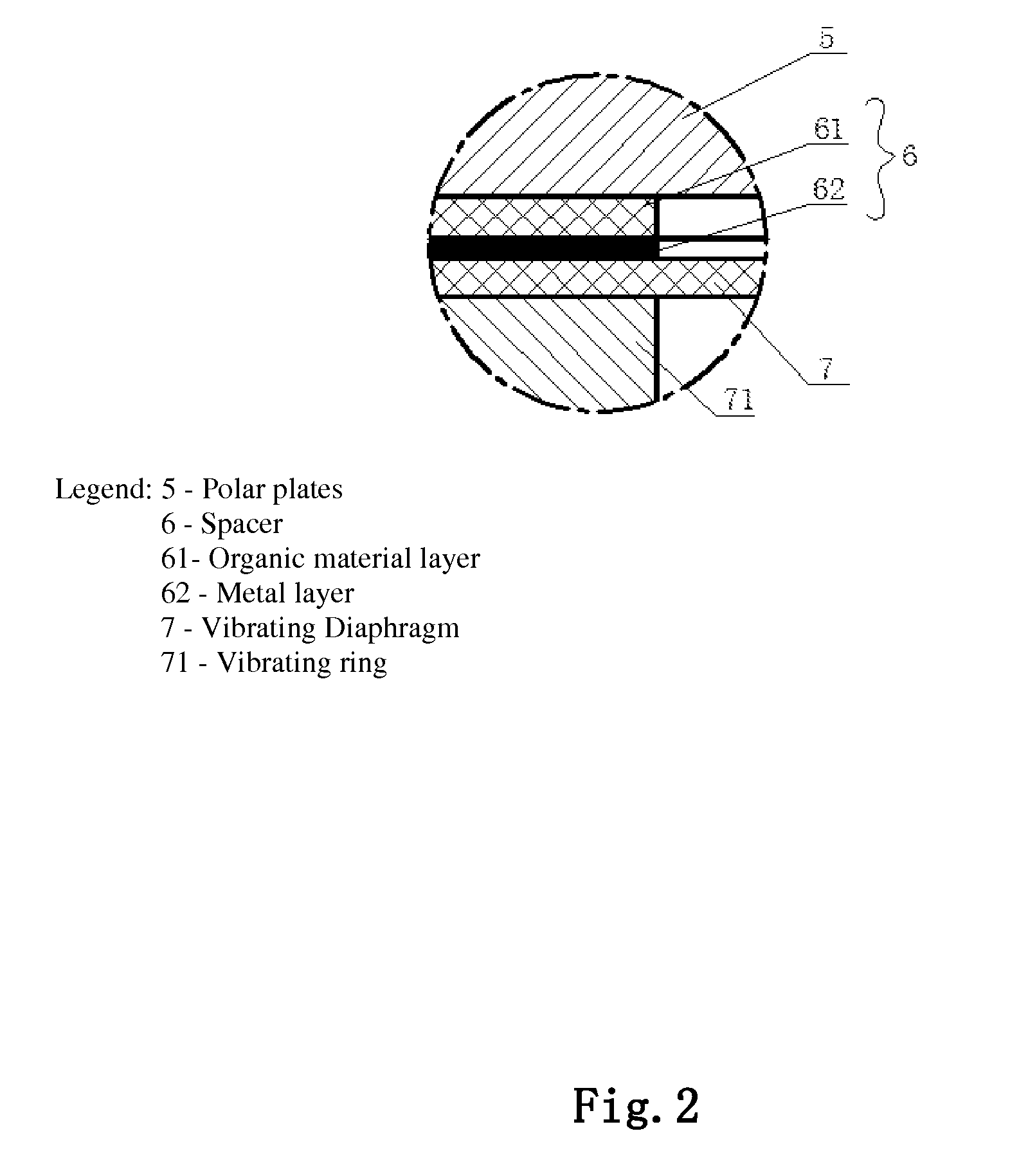
[0026]FIG. 1 is a cross-sectional view showing a specific structure of a capacitive microphone provided with the spacer according to the present invention. As shown in FIG. 1, the capacitive microphone with the spacer according to the present invention comprises a circuit board substrate 1 on the top, a circuit board base plate 3 on the bottom and a circuit board frame 2 between the circuit board substrate and the circuit board base plate, all or part of which may be fabricated from a circuit board and constitute a protection structure for the capacitive microphone. Here, a plurality of surface mountable electrodes 11 are provided on the top surface of the circuit board substrate 1 that faces outside of the microphone, and a signal amplification device 12 is provided on the bottom surface that faces inside of the microphone. In addition, a s...
second embodiment
[0030]The specific structure of the spacer according to the second embodiment of the present invention will be explained below. Compared with the structure of the first embodiment in which the spacer is comprised of a metal layer 62 and an organic material layer 61, the spacer of the second embodiment comprises two metal layers 62 located at outer levels and an organic material layer 61 sandwiched between these two metal layers. This structure may also realize effect similar to the first embodiment.
[0031]In addition, FIG. 5 shows another shape of the spacer 6 after modification, i.e. the spacer 6 is shaped as a square-shaped structure with an elliptic opening provided in the center. FIG. 6 shows the structure of a spacer array formed by connecting multiple spacers 6 shown in FIG. 5 together, wherein adjacent spacers 6 are connected via connecting sections 64 therebetween. Here, the connecting section 64 has an elongated strip shape extending along an edge of the spacer 6, and this s...
PUM
 Abstract
Description
Claims
Application Information


