Power lamp package

a power lamp and package technology, applied in the field of semiconductor device die package, can solve the problems of silver plated copper reflector tarnish, degraded reflective properties, adversely affecting the reflective capabilities of silver plated copper reflector and the light output of led packag

Active Publication Date: 2014-03-11
CREELED INC
View PDF253 Cites 13 Cited by
  • Summary
  • Abstract
  • Description
  • Claims
  • Application Information

AI Technical Summary

Problems solved by technology

It has been noted that the adhesive used to bond the reflector to the substrate may potentially cause the silver plated copper reflector to tarnish and its reflective properties to become degraded.
This in turn may adversely affect the reflective capabilities of the reflector and the light output of the LED package.

Method used


Image

  • Power lamp package
  • Power lamp package
  • Power lamp package

Examples


Embodiment Construction

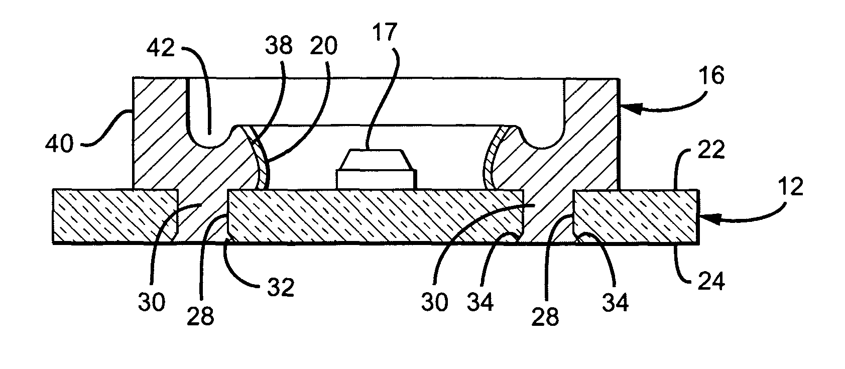
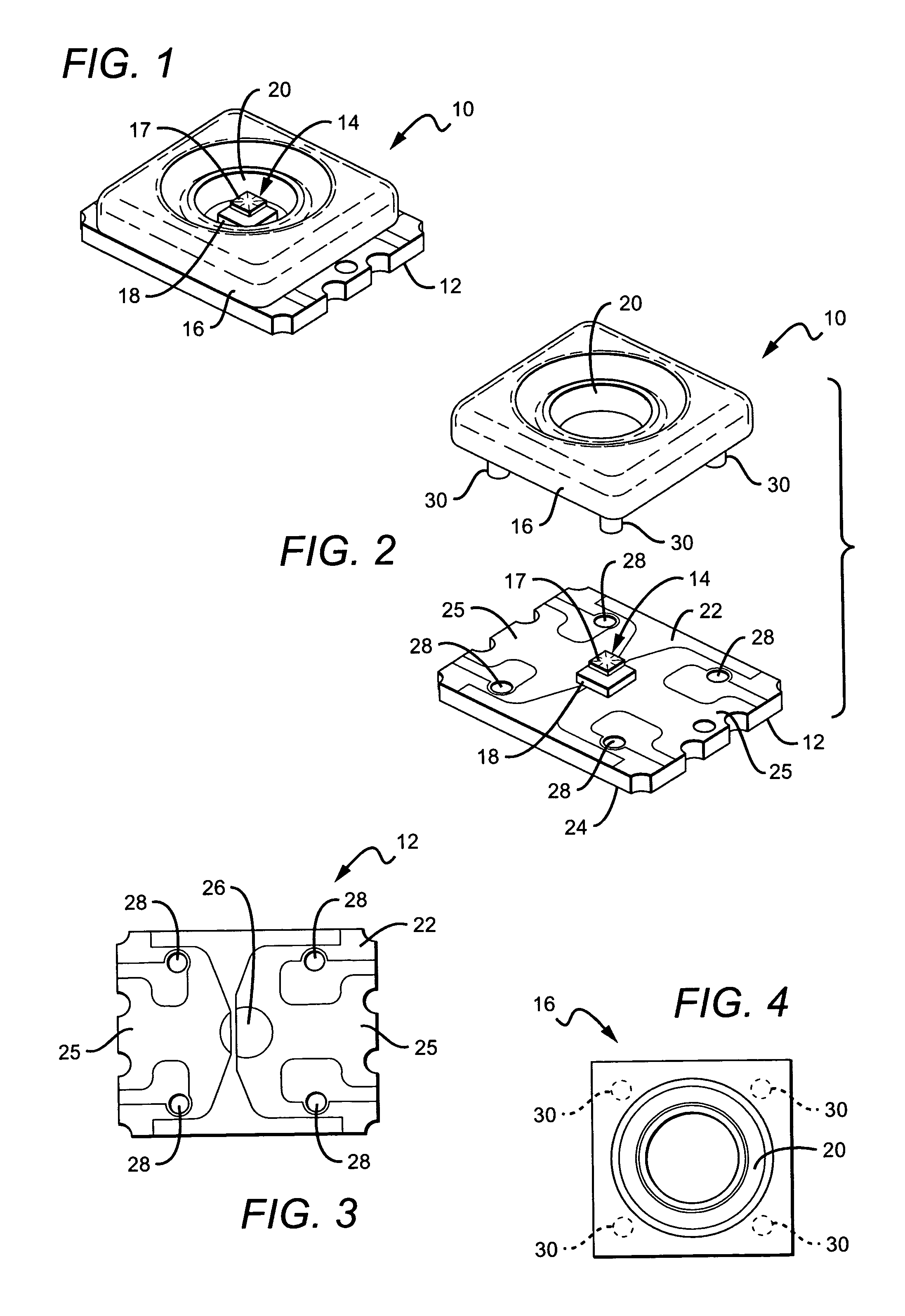
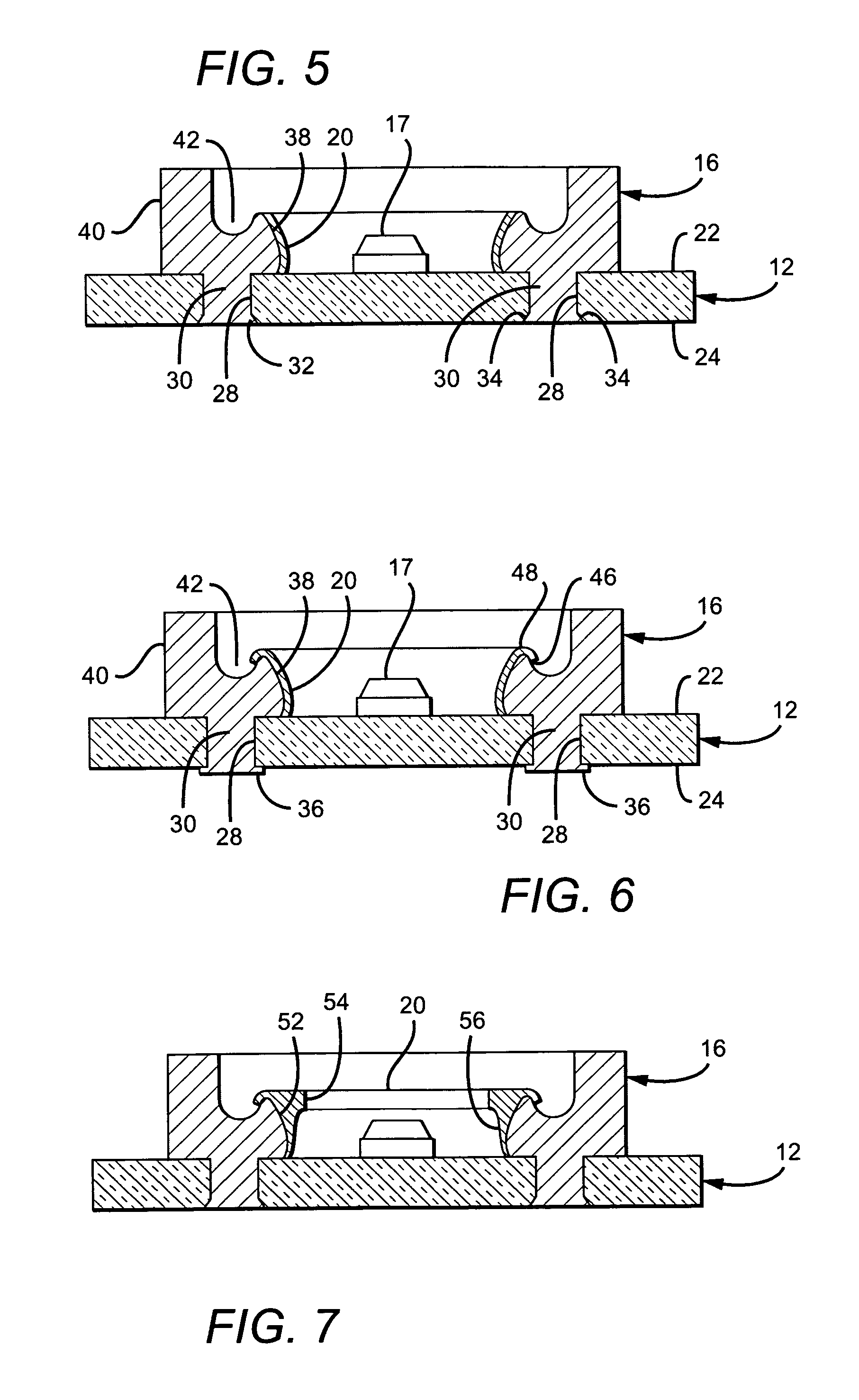
[0029]The present invention provides improved semiconductor die package performance through adhesive-free assembly of the substrate and reflector cup components of the package. In one embodiment, the reflector cup is injection molded onto a surface of the substrate and is held in place by adhesive free anchors. In another embodiment, the reflector cup is molded separate from the substrate and is secured in place on the substrate through various processes including deformation of a portion of the reflector cup such that the reflector cup is again held in place by adhesive free anchors. Portions of the reflector cup may be made reflective either by molding it from light reflective / scattering material or through the addition of a reflective element, such as a piece of foil material that is secured to the reflector preferably without the use of an adhesive. A variety of interchangeable reflective elements having different surface shapes, and thus different light reflecting properties, m...


PUM


Abstract

Adhesive-free assembly of the substrate and reflector components of a semiconductor die package is achieved by injection molding the reflector onto a surface of the substrate or by molding the reflector separate from the substrate and securing it in place on the substrate through deformation of a portion of the reflector. The reflector may be made reflective either by molding the reflector using a light scattering material or through the addition of a reflective element, such as a piece of foil material that is secured to the reflector. A variety of interchangeable reflective elements having different surface shapes, and thus different light reflecting properties, may be made.

Description

BACKGROUND OF THE INVENTION[0001]1. Field of the Invention[0002]This invention relates to semiconductor device die packages, and more particularly to light emitting diode (LED) die packages.[0003]2. Description of Related Art[0004]It is known to provide semiconductor light emitting devices, such as a light emitting diode (LED), in a package that may provide protection, color selection, focusing and the like for light emitted by the light emitting device (LED package). An LED package generally includes a substrate member on which a light emitting device is mounted. The light emitting device may, for example, include an LED chip / submount assembly mounted to the substrate member with electrical connections being made to the LED for applying an electrical bias. It is understood in the art that LEDs generally comprise an active region of semiconductor material sandwiched between two oppositely doped layers. When a bias is applied across the doped layers, holes and electrons are injected ...

Claims


Application Information

Patent Timeline
Patent Type & Authority Patents(United States)
IPC IPC(8): H01L33/48H01L33/60
CPCH01L33/60H01L33/486H01L2924/0002H01L2924/00
Inventor LEUNG, MICHAELIBBETSON, JAMES
Owner CREELED INC
Why Eureka
Try Eureka