AI technical title is built by Patsnap AI team. It summarizes the technical point description of the patent document.
a light-emitting diode and semi-polar technology, applied in the field of electroelectronic and optoelectronic devices, can solve the problems of increased wafer area, increased cost, and inability of car lamp assembly and illumination manufacturers to completely switch to led devices, and achieve the effect of reducing droop
Active Publication Date: 2014-04-01
RGT UNIV OF CALIFORNIA
View PDF25 Cites 4 Cited by
Summary
Abstract
Description
Claims
Application Information
AI Technical Summary
This helps you quickly interpret patents by identifying the three key elements:
Problems solved by technology
Method used
Benefits of technology
Problems solved by technology
As a result of droop, either more LED chips, or larger-area LED chips, are needed for high power devices, which results in increased wafer area and leads to higher costs.
For example, car lamp assembly and illumination manufacturers cannot completely shift to using LED devices because of their high cost.
Method used
Image
Click on the blue label to locate the original text in one second.
Reading with bidirectional positioning of images and text.
Examples
Embodiment Construction
[0042]In the following description of the preferred embodiment, reference is made to the accompanying drawings which form a part hereof, and in which is shown by way of illustration a specific embodiment in which the invention may be practiced. It is to be understood that other embodiments may be utilized and structural changes may be made without departing from the scope of the present invention.
Overview
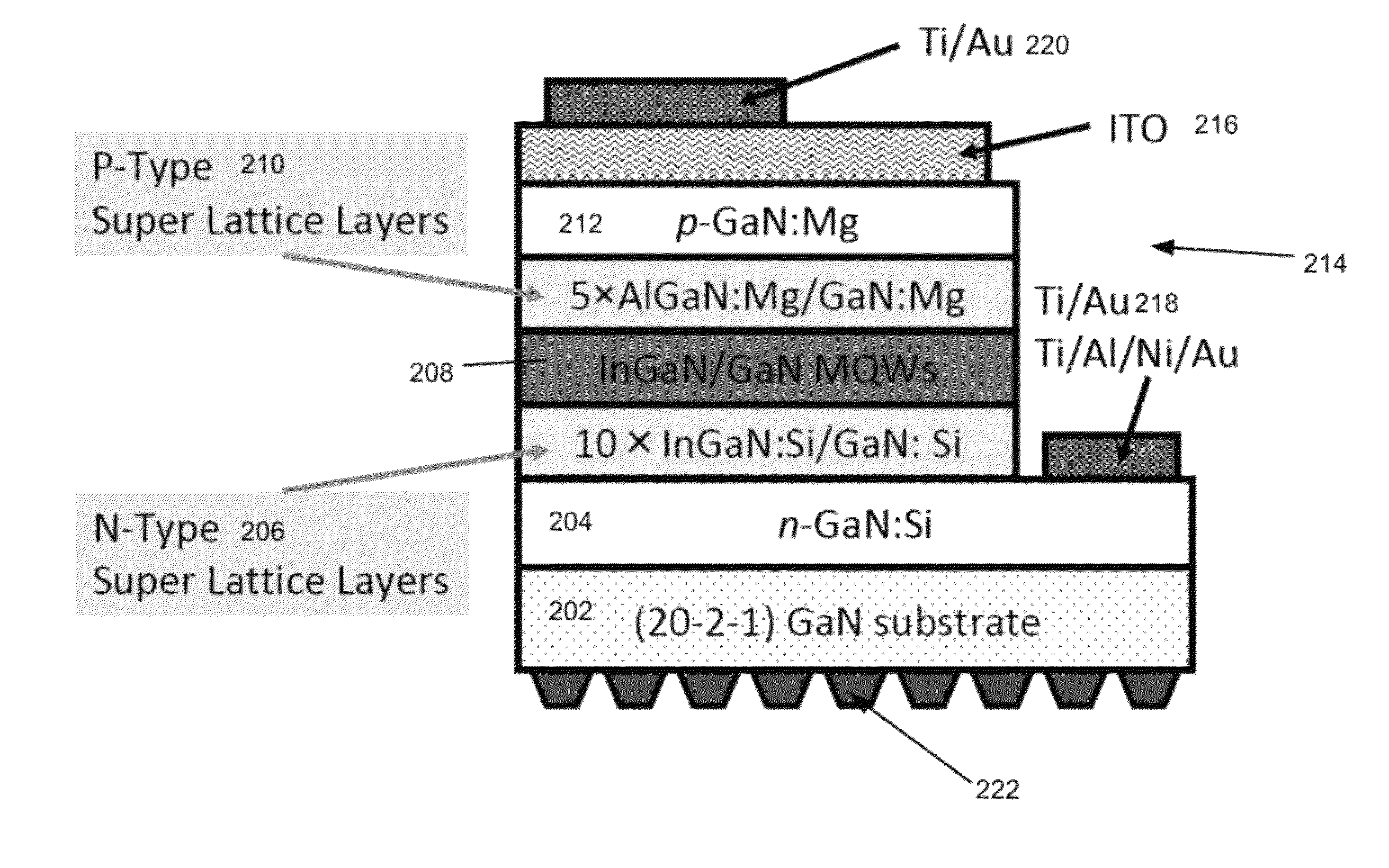
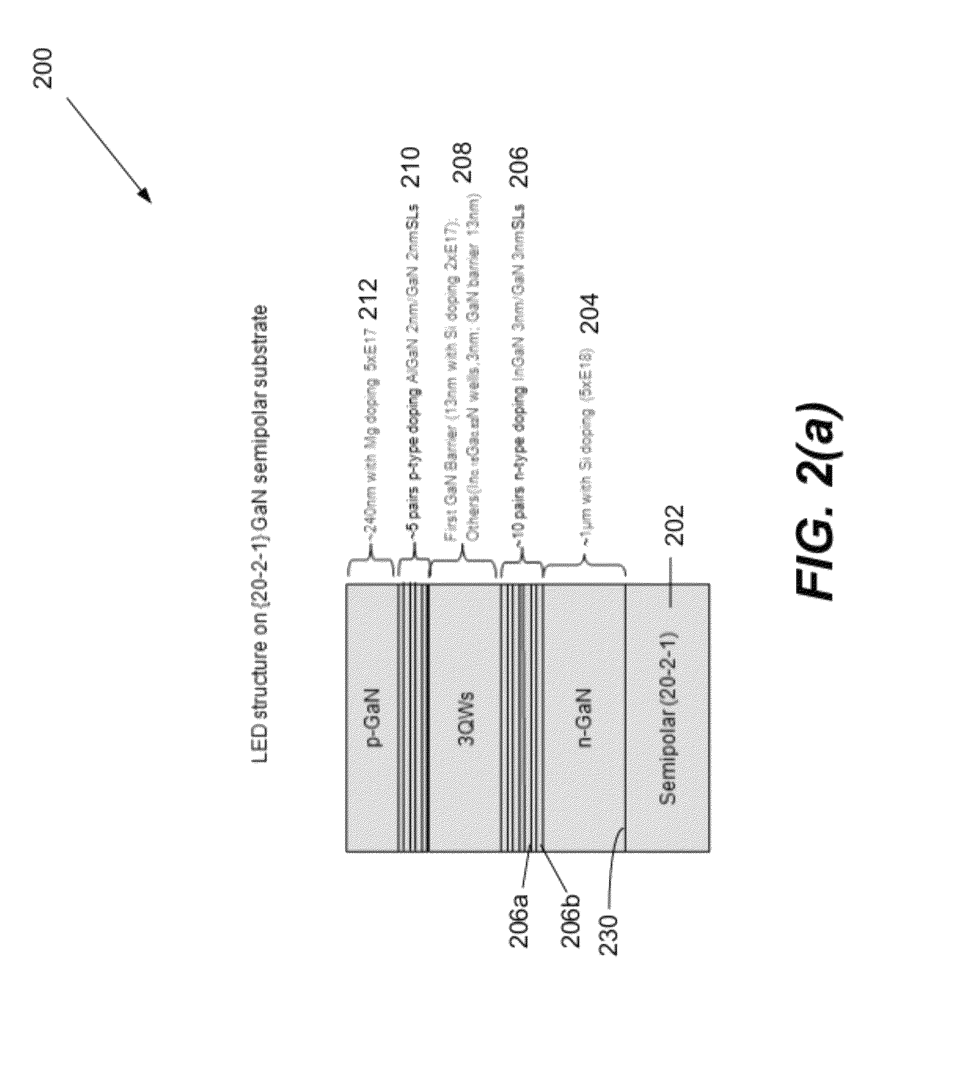
[0043]The present invention describes a LED structure comprising GaN thin films grown by MOCVD on GaN semipolar (e.g., {20-2-1}) substrates, for achieving low efficiency droop. The present invention provides a pathway to nitride-based devices free from the droop effect. The structure incorporates an n-SL located below the QWs, a QW active region of two or more periods, and more preferably, at least three periods, and a p-SL above the QWs. This structure shows reduced droop when incorporated into (Al,In,Ga)N devices grown on GaN semipolar (e.g., {20-2-1}) substrates.
[0044]On nonpolar...
PUM
Abstract
A light emitting diode structure of (Al,Ga,In)N thin films grown on a gallium nitride (GaN) semipolar substrate by metal organic chemical vapor deposition (MOCVD) that exhibits reduced droop. The device structure includes a quantum well (QW) active region of two or more periods, n-type superlattice layers (n-SLs) located below the QW active region, and p-type superlattice layers (p-SLs) above the QW active region. The present invention also encompasses a method of fabricating such a device.
Description
CROSS REFERENCE TO RELATED APPLICATION[0001]This application claims the benefit under 35 U.S.C. Section 119(e) of co-pending and commonly-assigned U.S. Provisional Patent Application Ser. No. 61 / 495,829, filed on Jun. 10, 2011, by Shuji Nakamura, Steven P. DenBaars, Shinichi Tanaka, Daniel Feezell, Yuji Zhao, and Chih-Chien Pan, entitled “LOW DROOP LIGHT EMITTING DIODE STRUCTURE ON GALLIUM NITRIDE SEMIPOLAR {20-2-1} SUBSTRATES,” which application is incorporated by reference herein.[0002]This application is related to co-pending and commonly-assigned U.S. Utility patent application Ser. No. 13 / 493,483, filed on same date herewith, by Shuji Nakamura, Steven P. DenBaars, Daniel F. Feezell, Chih-Chien Pan, Yuji Zhao and Shinichi Tanaka, and entitled “HIGH EMISSION POWER AND LOW EFFICIENCY DROOP SEMIPOLAR BLUE LIGHT EMITTING DIODES,” which application claims the benefit under 35 U.S.C. Section 119(e) of U.S. Provisional Patent Application Ser. No. 61 / 495,840, filed on Jun. 10, 2011, by ...
Claims
Application Information
Patent Timeline
Application Date:The date an application was filed.
Publication Date:The date a patent or application was officially published.
First Publication Date:The earliest publication date of a patent with the same application number.
Issue Date:Publication date of the patent grant document.
PCT Entry Date:The Entry date of PCT National Phase.
Estimated Expiry Date:The statutory expiry date of a patent right according to the Patent Law, and it is the longest term of protection that the patent right can achieve without the termination of the patent right due to other reasons(Term extension factor has been taken into account ).
Invalid Date:Actual expiry date is based on effective date or publication date of legal transaction data of invalid patent.

