Solar Cell Devices

a solar cell and cell technology, applied in the field of solar cell devices, can solve the problems of limiting the voltage of operation in the solar cell device, hampering the technical approach to high-performance solar photovoltaic devices, and limiting the conversion efficiency achieved in traditional single-junction semiconductor solar cells to less than 25%, so as to enhance the photovoltaic conversion efficiency of traditional semiconductor solar cells, enhance the performance of ingap/gaas/ge solar cells, and minimize manufacturing costs

Inactive Publication Date: 2010-01-14
KOPIN CORPORATION
View PDF6 Cites 95 Cited by
  • Summary
  • Abstract
  • Description
  • Claims
  • Application Information

AI Technical Summary

Benefits of technology

[0014]The solar cell device of the invention can enhance the photovoltaic conversion efficiency of traditional semiconductor solar cells while minimizing the manufacturing costs. In particular, the present invention employing quantum dots or wells embedded within the wide band gap matrix can enhance the performance of InGaP/GaAs/Ge solar cells currently used for space power. In addition, the present invention employing built-in quasi-electric fields ca

Problems solved by technology

The conversion efficiency achieved in traditional single-junction semiconductor solar cells is typically limited to less than 25%.
The voltage of operation in a solar cell device generally is also limited by the semiconductor band gap.
While these state-of-the-art multi-junction cells are suitable for some applications, fundamental issues often hamper this technical approach to high performance solar photovoltaic devices.
First, the current-matching requirements of series-connected devices make

Method used


Image

  • Solar Cell Devices
  • Solar Cell Devices
  • Solar Cell Devices

Examples


first embodiment

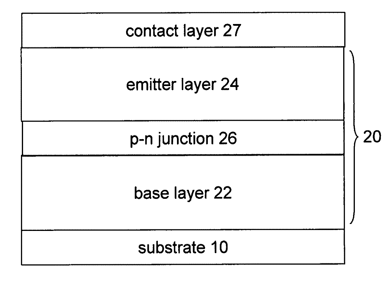
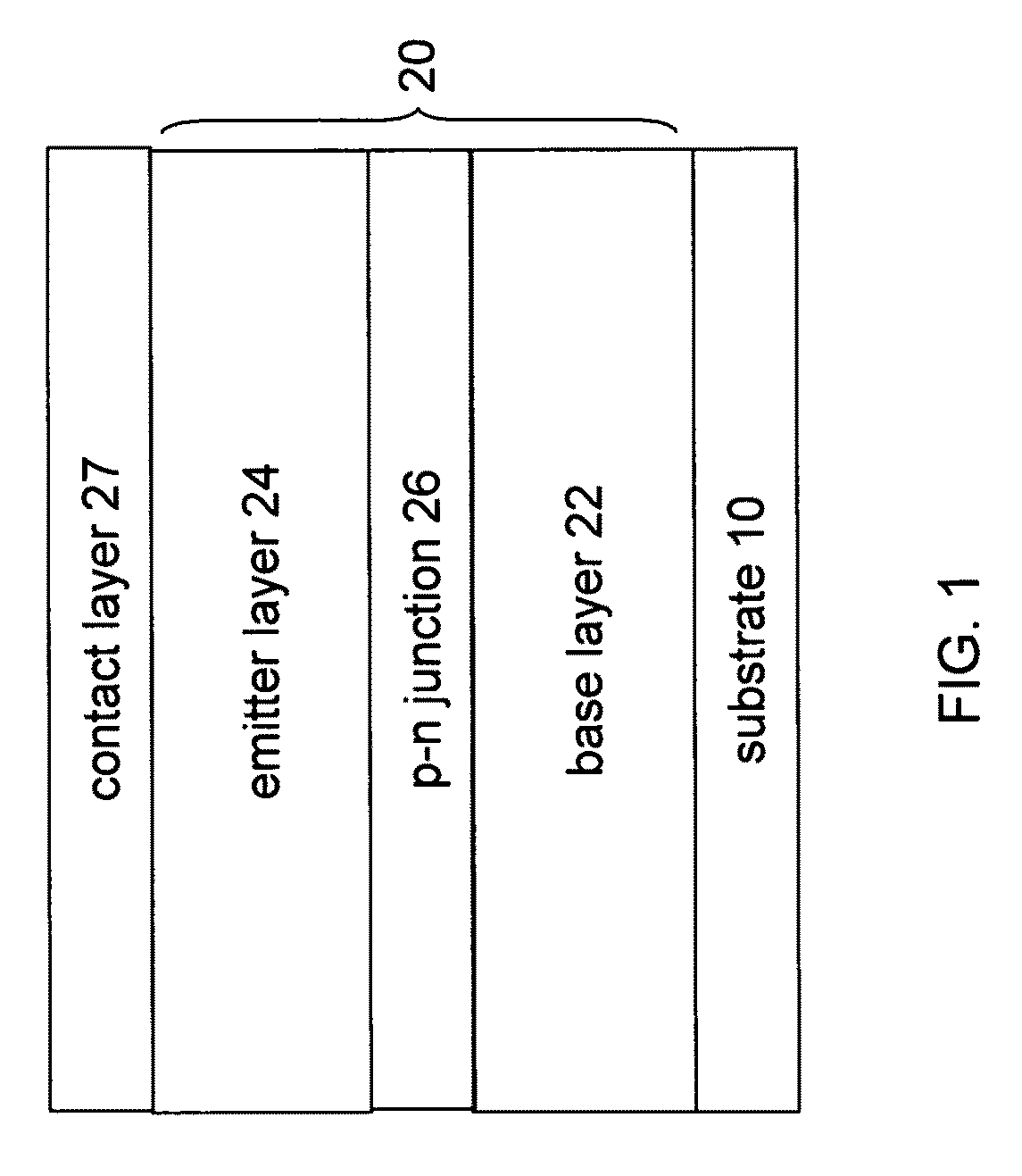
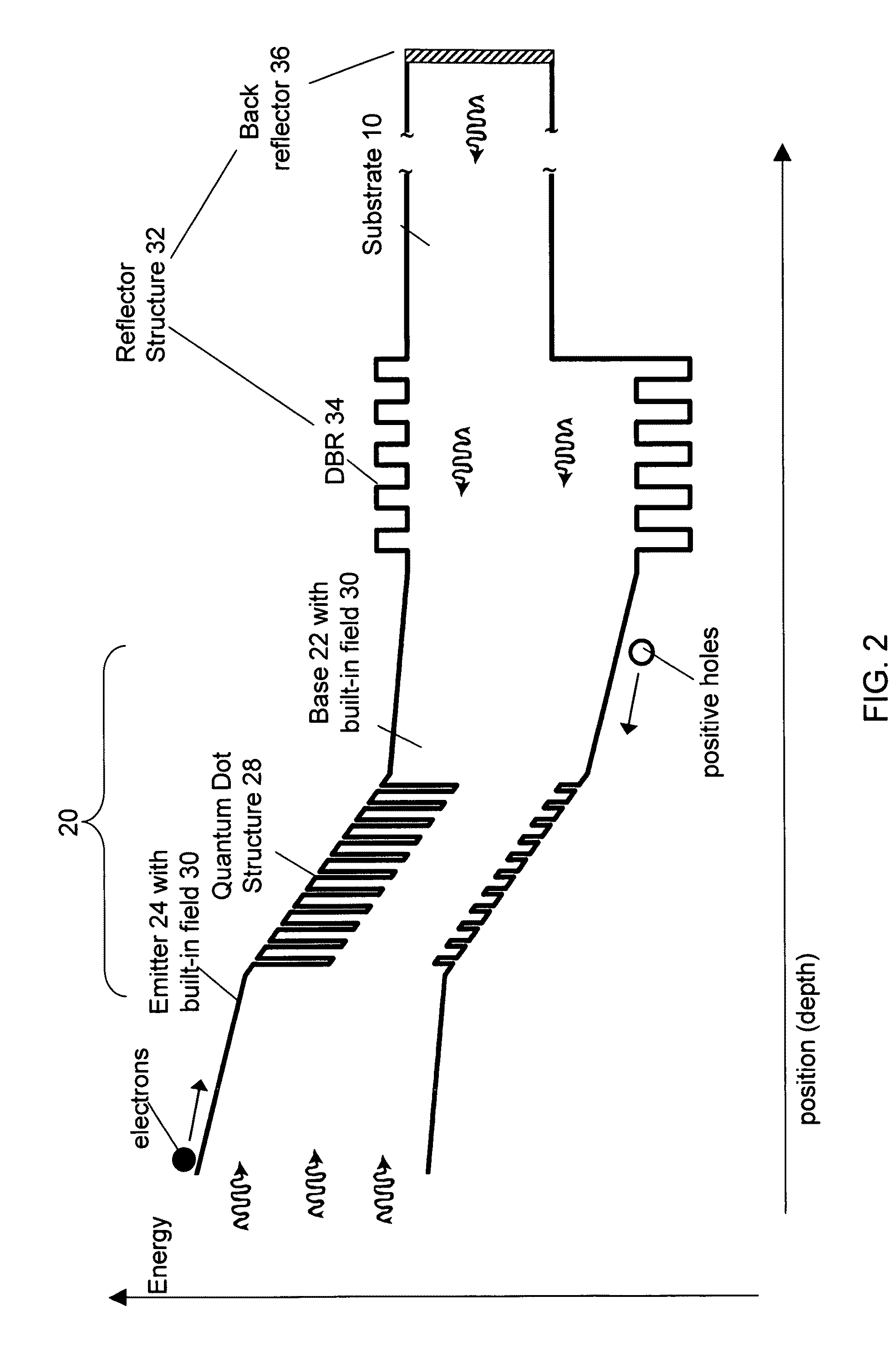
[0034]In a first embodiment, as shown in FIG. 2, a solar cell device of the invention further includes at least two features selected from: i) nano-structured region 28 at the p-n junction between base layer 22 and emitter layer 24 of at least one subcell, nano-structured region 28 including a plurality of quantum dots or quantum wells that are embedded within a band gap matrix that has a band gap greater than that of the quantum dots or the quantum wells embedded therein; ii) base layer 22 and / or emitter layer 24 of at least one subcell that includes either a compositional grade or a doping grade, or both, thereby having built-in quasi-electric field 30; and iii) photon reflector structure 32 between substrate 10 and p-n diode component 20, over substrate 10 and opposite p-n diode component 20, or over p-n diode component 20 and opposite substrate 10.

[0035]In a first aspect of the first embodiment, at least one subcell includes nano-structured region 28 at the p-n junction between ...

third embodiment

[0050]In yet another specific embodiment, photon reflector structure 32 includes one or more metallic layers. In yet another aspect of the third embodiment, photon reflector structure 32 includes one or more metallic layers, and is disposed over substrate 10 opposite p-n diode component 20. In these embodiments, specifically, substrate 10 includes GaP, ZnSe or ZnS.

[0051]In yet another specific embodiment, photon reflector structure 32 includes a distributed Bragg reflector (DBR) of AlAs, AlGaAs, AlGaInP, or AlInP. In yet another specific embodiment, photon reflector structure 32 includes a distributed Bragg reflector (DBR) of AlAs, AlGaAs, AlGaInP, or AlInP, and is disposed between substrate 10 and the p-n diode component 20.

[0052]In a fourth aspect of the first embodiment, nano-structured region 28, and base layer 22 that includes either a compositional grade or a doping grade, or both, thereby having built-in quasi-electric field 30, are employed. In a fifth aspect of the first em...

fourth embodiment

[0078]FIGS. 6A and 6B show one example of the FIG. 6A shows a cross-sectional view of a multi-junction solar cell of the invention. FIG. 6B shows the multi-junction solar cell of FIG. 6A in view of energy. In the device of FIGS. 6A and 6B, first subcell 50 and second subcell 52 are connected via tunnel junction 42. Alternatively, first subcell 50 and second subcell 52 can be each independently connected via a metal contact(s) (not shown in FIGS. 6A and 6B) instead of tunnel junction 42. Although only first and second subcells 50 and 52 are included in the device of FIGS. 6A and 6B, additional subcells can be added to the device of FIGS. 6A and 6B. Features, including specific features of, first and second subcells 50 and 52, and components thereof, are as described above, for example, with respect to FIGS. 2-5.

[0079]Suitable examples of materials for base layer 22 and emitter layer 26 of each of subcells 50 and 52 are as described above. Specifically, second subcell 52 includes a w...


PUM


Abstract

A solar cell device includes a p-n diode component over a substrate, the p-n diode component including at least one subcell, each subcell including an n-type semiconductor layer and a p-type semiconductor layer to form a p-n junction. The solar cell device further includes at least two features selected from: i) a nano-structured region between at the p-n junction of at least one subcell; ii) an n-type and/or a p-type layer of at least one subcell that includes a built-in quasi-electric field; and iii) a photon reflector structure. Alternatively, the solar cell device includes at least two subcells, and further includes a nano-structured region at the p-n junction of at least one of the subcells, wherein the subcells of the solar cell device are connected in parallel to each other by the p-type or the n-type semiconductor layer of each subcell. Alternatively, the solar cell device further includes a nano-structured region at the p-n junction of at least one subcell, wherein the nano-structured region includes i) a plurality of quantum dots or quantum wells that include InN or InGaN, the quantum dots or quantum wells embedded within a wide band gap matrix that includes InGaN, GaN, or AlGaN, or ii) a plurality of quantum dots or quantum wells that include InAs, GaAs or InGaAs, the quantum dots or quantum wells embedded within a wide band gap matrix that includes InGaP, GaAsP, AlGaAs, AlGaInAs or AlGaInP.

Description

RELATED APPLICATION[0001]This application claims the benefit of U.S. Provisional Application No. 60 / 926,325, filed on Apr. 26, 2007. The entire teachings of the above application are incorporated herein by reference.GOVERNMENT SUPPORT[0002]The invention was supported, in whole or in part, by a grant NNC07QA82P from the Small Business Technology Transfer (STTR) Program of the U.S. National Aeronautics and Space Administration (NASA). The Government has certain rights in the invention.BACKGROUND OF THE INVENTION[0003]Photovoltaic solar arrays provide an excellent source of power for commercial and military spacecraft and hold great promise as a sustainable, environmentally friendly energy source for the 21st century. While photovoltaics (PV) currently provide a minuscule percentage of the world's energy needs, it is a surprisingly large and rapidly growing industry. The worldwide PV market has been growing at over 30% annually since the late 1990s, and now generates well over $5 billi...

Claims


Application Information

Patent Timeline
IPC IPC(8): H01L31/06H01L31/0232H01L31/18
CPCB82Y20/00H01L31/03046Y02E10/544H01L31/035281H01L31/1035H01L31/035236Y02P70/50
Inventor WELSER, ROGER E.
Owner KOPIN CORPORATION
Why Eureka
Try Eureka